Choose timezone
Your profile timezone:
The conference will take place at Hotel Hermitage, La Biodola Bay, Isola d'Elba (Italy) from the 15th (arrival date) to the 20th (departure date) of May 2022.
PLEASE NOTE: the Conference registration is closed, please write an email to leaps2022@lists.lnf.infn.it if you are interested to participate
LEAPS is the League of European Accelerator-based Photon Sources, a strategic consortium initiated by the Directors of the Synchrotron Radiation and Free Electron Laser (FEL) user facilities in Europe. Its primary goal is to actively and constructively ensure and promote the quality and impact of the fundamental, applied and industrial research carried out at their respective facility to the greater benefit of European science and society.
In this context LEAPS will organize in May 15 - 20, 2022 the first LEAPS Topical Conference aiming to bring together the latest achievements from the synchrotron radiation user community with those from source development and instrumentation. The focus of the first LEAPS Conference will be dedicated to the opportunities emerging from the Quantum Technologies R&D. This conference shall showcase where today and future synchrotron radiation contributes to the advancements of Quantum Technologies.
This Conference will be by invitation after the pre-registration. Registration forms will be moderated.
A conference fee will be requested for participation.

INSTRUMENTATION TUTORIAL
TUTORIAL
TUTORIAL
INSTRUMENTATION TUTORIAL
Photoemission with angular and spin resolution (Spin-ARPES) probes directly the electronic bands and their spin textures in solids. The development of the technique is closely related to, and stimulated by the development of novel quantum materials, often characterized by peculiar spin arrangements. We developed a highly efficient Spin-ARPES spectrometer [DOI:10.1107/S1600577517006907] hosted at the APE-LE beamline (Elettra/NFFA facilities), which became one of the reference European Spin-ARPES setups, heavily exploited in the investigation of novel candidate spintronic materials.
Here I will show how we implemented Spin-ARPES in the investigation of Dirac semimetals that attract attention due to the considerable technological potential related to their nontrivial topological states and exotic quantum transport. Especially, materials hosting type-II Dirac fermions are expected to provide functionalities enabled by anisotropic optical and magnetotransport properties. Nevertheless, any practical implementation remained elusive so far since the Dirac point lies far from the Fermi level, limiting the technological exploitation. By means of spin-ARPES we found that kitkaite NiTeSe hosts both the type-II bulk Dirac fermions and the topological spin polarized surface states in close proximity of the Fermi level and this likely plays a role in the performance of NiTeSe-based microwave detector that was subsequently demonstrated [DOI:10.1002/adfm.202106101].
Moore-ruled down-scaling of magnetic bits in new-generation memories hampers deterministic switching and calls for new techniques for magnetization manipulation. Acoustic control of magnetism is an appealing route for low-energy-consumption operation, e.g. exploiting magneto-elastic coupling (MEC) in a thin-film planar heterostructure, where SAWs at micron-size wavelength drive magnetization precession by inverse magnetostriction [1].
We studied MEC in Nickel films (8-40 nm) deposited on amorphous and crystalline substrates. We employed a four-wave-mixing approach [2] in a UHV-ready TG-spectroscopy setup, with a 300 fs, high frequency laser (NFFA-SPRINT*). Two pump pulses thermally excite SAWs, which couple to magnetostatic waves. A third time-delayed pulse acts either as acoustic (TG diffraction), or as magnetic probe (Faraday rotation). Tuning an external magnetic field, the condition of SAW-driven ferromagnetic resonance (FMR) is reached: the time-dependent magneto-elastic field balances the Gilbert damping, allowing spin precession to last long after its natural damping. The range of wavevectors studied (few inverse microns) allows a comparison with results from standard FMR in terms of Kittel curve and extrinsic contribution to the magnetic damping.
*https://www.trieste.nffa.eu/techniques/spectroscopy/tg-sprint/
[1] W.Yang and H.Schmidt, Appl.Phys.Rev. 8, 021304 (2021)
[2] J.Janušonis et al. Sci.Rep. 6.1, 1-10 (2016)
Identifying an efficient pathway to change the order parameter via a subtle excitation of the coupled high-frequency mode is the ultimate goal of the field of ultrafast phase transitions. This is an especially interesting research direction in magnetism, where the coupling between spin and lattice excitations is required for magnetization reversal. Despite several attempts however, the switching between magnetic states via resonant pumping of phonon modes has yet to be demonstrated.
To provide strong resonant excitation of the phonon modes, we use pulses from FELIX (Free Electron Laser for Infrared eXperiments, Nijmegen, The Netherlands). The IR/THz light with photon energy ranging between 25 meV and 124 meV (wavelength 10-50 $\mu$m) is typically used, with pulse energy between 20 $\mu$J in a single micropulse, and 150 $\mu$J using cavity-dumping.
And thus we show how an ultrafast resonant excitation of LO phonons in magnetic garnet films switches magnetization into a peculiar quadrupolar magnetic domain pattern, unambiguously revealing the magneto-elastic mechanism of the switching. In contrast, the excitation of strongly absorbing TO modes results in thermal demagnetization only. The mechanism appears to be very universal, and is shown to work in samples with very different crystallographic symmetry and magnetic properties, such as antiferromagnets.
Silicon, a ubiquitous material in modern computing, is an emerging platform for realizing a source of indistinguishable single-photons on demand. The integration of recently discovered single-photon emitters in silicon into photonic structures is advantageous to exploit their full potential for integrated photonic quantum technologies [1] [2]. Here, we show the integration of telecom photon emitters in a photonic platform consisting of silicon nanopillars. We developed a CMOS-compatible nanofabrication method, enabling the production of thousands of individual nanopillars per square millimetre with state-of-the-art photonic-circuit pitch, all the while being free of fabrication-related radiation damage defects. We found a waveguiding effect of the 1278 nm G-center emission along individual pillars accompanied by improved brightness, photoluminescence signal-to-noise ratio and photon extraction efficiency compared to that of bulk silicon. These results unlock clear pathways to monolithically integrating single-photon emitters into a photonic platform at a scale that matches the required pitch of quantum photonic circuits.
[1] Hollenbach M., Berencén Y. et al. "Engineering telecom single-photon emitters in silicon for scalable quantum photonics", Opt. Express 28, 26111-26121 (2020)
[2] Redjem W., Durand, A., Herzig, T. et al. "Single artificial atoms in silicon emitting at telecom wavelengths", Nat. Electronics 3, 738–743 (2020)
The present poster shows current results we obtained concerning the dynamics of quantum correlations in two noninteractive 2-level atoms coupled to two independently identical thermal reservoirs. The atoms were initially prepared in a Gisin state, which is a mixture of a maximally entangled two-qubit state and a separable mixed state. The quantum entanglement in the evolved Gisin state is quantified by logarithmic negativity (LN), and the nonclassical correlation is characterized by trace distance discord (TDD) and local quantum uncertainty (LQU). Using the mean photon number of reservoirs and spontaneous emission rates of atoms as inputs, we examine how these quantum correlation quantifiers behave. According to our study, trace distance discord (TDD) is the most effective quantifier for revealing nonclassical correlations in the two 2-level system induced by the interaction with thermal reservoirs in all scenarios.
In this presentation I will show the actual state-of-the-art of our Nitrogen Vacancy center in diamond (NV) platform and develop a theoretical and phenomenological model to evaluate the expressions for the probability p(n,t) that n photons are spontaneously emitted in a given time t by a NV under non-resonant excitation from a 532nm laser and resonant MW radiation. This allows for a better understanding and characterization of this important quantum system and can be extended to other quantum defects, such as SiC. These results pave the way for optimized protocols to enhance the sensitivity and coherence of these quantum platforms for quantum sensing and quantum computing.
Superconductivity in group IV semiconductors is desired for hybrid devices combining both semiconducting and superconducting properties. Following boron-doped diamond and Si, superconductivity has been observed in gallium-doped Ge; however, the obtained specimen is in polycrystalline form [Phys. Rev. Lett. 102, 217003 (2009)]. Here we present superconducting single-crystalline Ge hyperdoped with gallium or aluminum by ion implantation and rear-side flash lamp annealing. The maximum concentration of Al and Ga incorporated into substitutional positions in Ge is 8 times higher than the equilibrium solid solubility. This corresponds to a hole concentration above 1021cm−3. Using density functional theory in the local-density approximation and pseudopotential plane-wave approach, we show that the superconductivity in p-type Ge is phonon mediated. According to the ab initio calculations, the critical superconducting temperature for Al- and Ga-doped Ge is in the range of 0.45 K for 6.25at.% of dopant concentration, being in qualitative agreement with experimentally obtained values. Being Si-chip technology compatible, superconducting Ge can find wide applications in quantum technology.
Electron spins in Si/SiGe heterostructures are promising for large-scale integration of solid state qubits in a CMOS compatible material system. A key requirement for realizing large arrays of qubits with shared gate control is a high degree of homogeneity of the strain in the Si quantum well (QW) hosting the qubits. Local inhomogeneities in the crystal lattice affect the band structure the QW and the qubit properties. Here, we use Scanning Xray Diffraction Microscopy (SXDM) to investigate non-destructively the lattice homogeneity in a qubit device based on a Si/SiGe heterostructure. We quantify all components of the strain and rotation tensors by combining SXDM datasets and find local variations on the order of 1e-4. These fluctuations are assumed to be caused by dislocation bunching and the thermal contraction of the gate electrodes. The data is compared to thermomechanical simulations showing a complex depth profile of elastic interaction. We find that the resulting variations of the electron band structure are on the same order of magnitude as the typical charging energy of an electrostatic quantum dot of ca. 1 meV. This indicates that structural inhomogeneities must be taken into account in the optimization of a SiGe-based qubit architecture for quantum computing.
Hybrid systems consisting of semiconductor channels and superconducting elements allow the formation of Andreev qubits and are therefore among the novel material platforms which could pave the way to scalable quantum computation. A key ingredient to achieve high coherence time and strong qubit-qubit coupling is the establishment of a clean superconductor / low-D semiconductor interface and highly transparent channels. To this aim, InAs 2D electron gases (2DEGs) are the ideal semiconductor systems due to their vanishing Schottky barrier; however, their exploitation is limited by the non-availability of commercial lattice-matched substrates.
We show that in-situ growth of superconducting aluminum on near-surface InAs metamorphic 2DEGs can be performed by Molecular Beam Epitaxy on GaAs substrates with state-of-the art quality, despite the 7% InAs/GaAs lattice mismatch. 2DEGs down to 10nm from the surface showed record-high low-T electron mobilities, and well-developed Quantum Hall and Quantum Point Contact features.
Al growth resulted in crystalline thin films with the coexistence of different crystallographic domains. Resistivity as a function of temperature was comparable to the best Al layers on GaAs and superconducting proximity effect was observed in a Josephson junction. The observed phenomenology opens the way to the exploitation of Andreev physics on our platforms.
Recent years witnessed various supervised learning frameworks relying on trainable quantum circuits as a result of advancement of quantum machine learning. The variational quantum classifier classifies data using a Variational Quantum Circuit (VQC) with an ansatz. The primary goal of the quantum supervised learning classifiers is to use the quantum feature map to transform data from distinct classes to different places in Hilbert space. However, it is not feasible to do feature selection beforehand, and for high-dimensional data using specific features to embed in the ansatz leads to data loss and error in classification. Hence, often data reduction technique like Shannon map is used on the data before uploading it to the quantum circuit. To obviate the data reduction before feeding to the circuit, dense parameterized quantum circuits with lesser number trainable parameters have been proposed without compromising the classification accuracy. The proposed quantum supervised learning framework is an improvement over established work on supervised quantum classifications. To show the effectiveness of the proposed densed quantum circuit, extensive experiments have been performed on IRIS data set and results show that it outperforms the previous quantum supervised classification frameworks in terms of classifications accuracy and complexity of the frameworks.
We analyse the implementation of a fast nonadiabatic CZ-gate through the resonance between the $|11\rangle$ and $|20\rangle$ states of transmon qubits with tunable coupling. We explicitly derive an effective Hamiltonian for the low-energy eigenstates. This allows us to identify different sources of error and design controls based on the theory of dynamical invariants, which has been proven to be particularly attractive due to their reduced leakage and robustness against decoherence. Our results show that these protocols achieve gate fidelities higher than the fast quasiadiabatic dynamics within times that approach the theoretical limit. This study paves the way for large-scale implementation of high-fidelity quantum operations.
Complex oxides host a multitude of novel phenomena in condensed matter physics, such as various forms of multiferroicity, colossal magnetoresistance, quantum magnetism and superconductivity. Defect engineering via ion irradiation can be a useful knob to control these physical properties for future practical applications. Two prominent effects are disorder and uniaxial strain. Particularly, the uniaxial strain, manifesting as the elongation of the out-of-plane lattice spacing, is not limited to available substrates. In this contribution, we will take SrRuO3 thin films as an example to show the emerging properties upon defect engineering by ion irradiation. The irradiated SRO films exhibit a pronounced topological Hall effect in a wide temperature range from 5 to 80 K. It can be attributed to the emergence of Dzyaloshinskii–Moriya interaction as a result of artificial inversion symmetry breaking associated with the lattice defect engineering. Ion irradiation has been well developed for semiconductor-chip technology and is readily applicable for all kinds of oxide quantum materials.
Single-photon sources are one of the elementary building blocks for photonic quantum information and optical quantum computing [1]. One of the upcoming challenges is the monolithic photonic integration and coupling of single-photon emission, reconfigurable photonic elements and single-photon detection on a silicon chip in a controllable manner. Particularly, fully integrated single-photon emitters on-demand are required for enabling a smart integration of advanced functionalities in on-chip quantum photonic circuits [2].
This work presents a mask-free nanofabrication method involving a quasi-deterministic creation of scalable extrinsic color centers in silicon emitting in the optical telecom O-band [3] on a commercial silicon-on-insulator platform using focused ion beam writing. We also show the local writing of an intrinsic color center in silicon, which is linked to a tri-interstitial complex and reveals quantum emission close to the telecom band [4]. The successful integration of these telecom quantum emitters into photonic structures such as micro-resonators, nanopillars [5] and photonic crystals with sub-micrometer precision paves the way toward a monolithic, all-silicon-based semiconductor-superconductor quantum circuit.
[1]D. D. Awschalom et al.,Nature Photonics 12,516 (2018)
[2]J. C. Adcock et al.,IEEE, 27, 2, (2021)
[3]M. Hollenbach et al.,Optics Express 28,26111 (2020)
[4]Y. Baron et al.,arXiv:2108.04283 (2021)
[5]M. Hollenbach et al.,arXiv:2112.02680 (2021)
n-type doping of Si by the deep chalcogen donor Te in excess of the solubility limit was recently demonstrated to lead to hyperdoped material [1]. Our investigation by hard x-ray photoelectron spectroscopy (hXPS) reveals at least two different Te species with different binding energy and systematically varying concentrations with increasing ion implantation dose. At the highest doping we study the photoelectron scattering patterns using hard x-ray photoelectron diffraction (hXPD) [2]. Substitutional site occupation of both Te monomers as well as dimers is identified with increasing binding energy leading to the main features in the XPS spectra. The sharp hXPD patterns allow the detailed analysis of the local surrounding of the dopant atoms [3]. At the lowest binding energy, an additional species is found and the distinct, rather diffuse hXPD pattern at this binding energy suggests the assignment of this component to a small fraction of Te in clusters.
References
[1] M. Wang et al. Phys. Rev. Appl. 11 054039 (2019) and references therein.
[2] O. Fedchenko et al NJP 21, 113031 (2019); [3] O. Fedchenko et al NJP 22, 103002 (2020).
The diamond anvil cell (DAC) is the tool that allows scientists to create pressures comparable to those existing in the Earth core, above the megabar. These conditions lead to new states of matter with specific magnetic and superconducting properties. However, the minute size of the sample and the constraints associated to the DAC make the implementation of magnetic diagnostics highly challenging. We will report the realization of an optical magnetometry technique that can detect the sample magnetic behavior through the diamond anvil, based on Nitrogen-Vacancy (NV) centers located at the surface of the anvil.
The NV center has a spin-dependent photoluminescence. By combining a microwave excitation and an optical excitation/readout, we can reconstruct the full vector magnetic field inside the diamond anvil cell at pressures as high as 60 GPa so far. Furthermore, the relatively simplicity of the setup enables its transportation and use on a synchrotron beamline
As a proof-of-principle, we detected the α-ε phase transition of iron with pressure through the monitoring of its magnetization, while simultaneously following the crystalline phase transition via X-ray diffraction. We will also report experiments performed on MgB2 that demonstrate the detection of a superconducting state through the observation of the Meissner effect.
INSTRUMENTATION TUTORIAL B
On the wake of the results obtained so far at the SPARC_LAB test-facility at LNF, we are currently in the process to design and build a new multi-disciplinary user-facility, equipped with a soft X-ray Free Electron Laser (FEL) driven by a ~1 GeV high brightness linac based on plasma accelerator modules. It is widely accepted by the international accelerator scientific community that a fundamental milestone towards the realization of a plasma driven future Linear Collider (LC) will be the integration of the new high gradient accelerating plasma modules in a FEL user facility (see the H2020 approved Design Study EuPRAXIA). This fundamental goal will be integrated in the LNF facility by using a high gradient X-band RF linac and the high power laser FLAME to drive Plasma Oscillations in the accelerator module. This activity is performed in the framework of the EuPRAXIA design study. In this talk we report about the recent progresses in the on going design study of the new facility and about opportunities and perspectives for international FEL user community.
At three end stations at BESSY II with cutting-edge angle-resolved photoemission spectroscopy (ARPES) instruments, we are able to study various electronic properties of quantum materials due to the versatile functions of our end stations. ARPES 1^3 station provides the highest energy resolution (~1 meV) at ultimately low sample temperatures (~1 K). ARPES 1^2 station allows for a broad exploration of reciprocal space and has versatile sample handling and preparation facilities. The Spin-ARPES system can detect the three components of the spin polarization vector with high energy and momentum resolutions. Here, we give examples from our recent work on three different material systems done at BESSY II: 1. Superconducting gap in the kagome superconductor CsV3Sb5. 2. Magnetic gap at the Dirac point in the topological insulator heterostructure system of Bi2Te3/MnBi2Te4 3. New type of Fermi arc in the antiferromagnet NdBi.
We will discuss several experimental approaches of imaging the band structure by ARPES and spin-polarized ARPES. We will consider various energy ranges from x-rays [1] to 6 eV [2], and various materials, from bulk crystals [1] to ultrathin films [2] and exfoliated atomically-thin flakes [3]. We will discuss technical aspects such as the angular and energy resolution, depth sensitivity, and various modes of adding spin-sensitivity to ARPES. We will compare the parameters of several synchrotron-based ARPES, micro-ARPES and spin-APRES machines, to our lab-based laser-driven high-resolution spin-ARPES system equipped with the exchange scattering spin detector. We will also discuss how to establish an intuitive relation between the initial state orbital and spin textures, and the dichroic and spin textures measured in the ARPES map, through the analysis of the photoemission matrix elements. This relationship is one of the necessary links to establish the connection between the band structure mapping and topological magneto-transport properties of novel materials.
[1] A. X. Gray et al., Nature Materials 11, 957 (2012)
[2] R. C. Vidal et al., Phys. Rev. Lett. 126, 176403 (2021)
[3] E. Mlynczak et al., Phys. Rev. B 103, 035134 (2021)
[4] M. Gehlmann et al., Nano Letters, 17, 5187 (2017)
We investigate the spin dynamics driven by terahertz magnetic fields in epitaxial thin films of
cobalt in its three crystalline phases. The terahertz magnetic field generates a torque on the magnetization which causes it to precess for about 1 ps, with a sub-picosecond temporal lag from the driving force. Then, the magnetization undergoes natural damped THz oscillations at a frequency characteristic of the crystalline phase (see fig. 1). We describe the experimental observations solving the inertial Landau-Lifshitz-Gilbert equation. Using the results from the relativistic theory of magnetic inertia, we find that the angular momentum relaxation time η is the only material parameter needed to describe all the experimental evidence. Our experiments suggest a proportionality between η and the strength of the magneto-crystalline anisotropy.
BOREAS beamline 29 at ALBA Synchrotron Light Facility is a soft X-ray beamline dedicated to polarization-dependent spectroscopic investigations of advanced materials, enabling techniques such as x-ray magnetic circular and linear dichroism (XMCD, XMLD), and soft x-ray resonant scattering (including reflectometry, gisaxs, holography and coherent imaging) [Barla et al., J. Synchrotron Rad. 23,1507 (2016)]. The beamline provides a rather broad photon energy range (80 eV to above 4000 eV) with full polarization control for experiments at two endstations for spectroscopy and scattering approaches, both implementing high field (6 and 2 Tesla) and low temperature capabilities (4-380 K and 18-400K). This allows atomic level investigation of magnetic and electronic properties of quantum materials, among which ferromagnets, antiferromagnets, superconductors, ferroelectrics, multiferroics or topological insulators. Investigated samples have the form of isolated atoms, nanoparticles and powders, organic molecules, van-der-waals layers, thin films or bulk specimens. Operative since mid 2012, along the past few years we have largely enhanced the instrumentation available In this contribution, we will provide details on the new available instrumentation, highlights of recent experiments, and outline some ideas for the future upgrade of the instrumentation in the frame of ALBA II project and the evolution of the scientific context.
LOREA, the ninth beamline of the ALBA synchrotron radiation source, started its operation in 2021 and is dedicated to electronic structure investigation of quantum materials by means of Angle Resolved Photo-Emission Spectroscopy (ARPES).
The photon energy range of the beamline (10-1000 eV) with continuously variable polarization and resolving power of more than 10ˆ4 in the whole range allows the complete characterisation of samples. A small spot size of about 10x10 μmˆ2 and the presence of 4 electrical contacts in the sample stage enables LOREA to characterise very small samples and simple devices.
The ARPES detector is an MBS A-1 hemispherical analyzer with very high energy and angular resolution (better than 1meV and 0.1˚) and the fast Fermi surface mapping mode. It will be upgraded in 2022 with a spin detector to perform spin-resolved ARPES.
The 6-axes cryo-manipulator can reach temperatures lower than 7.5K.
The main chamber is connected to a central radial distribution chamber and, through it, to all other vessels, including chambers for in situ UHV deposition and characterization, load lock and sample storage, docking of vacuum suitcase.
This project is co-funded by the European Regional Development Fund (ERDF) within the “Framework of the Smart Growth Operative Programme 2014-2020”
A high-temperature superconducting (HTS) undulator is under development at the Paul Scherrer Institut. This device equipped with HTS bulks is a novel technology to generate short period and high strength magnetic field. For medium-energy synchrotron storage rings, this is a promising option to increase tremendously the photon flux in hard X-ray domain. The experiment for a sample consisting of 20 HTS bulks gave an encouraging result above 1.9 T magnetic field of 10-mm period at 4-mm magnetic gap. Nevertheless, the peak-to-peak fields are not homogeneous enough to ensure the corresponding photon beam quality. A magnetic optimization method of sorting and shimming is presented together with the simulation of the resulting optimized field.
Mammalian Rhodopsin, a prototype of the largest druggable G Protein-Coupled Receptors family (GPCRs), is our light receptor for night vision. Upon photon absorption, its chromophore 11-cis retinal undergoes one of the fastest events in biology, which happens in the femtosecond range, the isomerization into the agonist form, all-trans retinal. We have developed a new crystal form of rho-dopsin, diffracting to better than 2 Å, which is suitable for room temperature time-resolved serial crystallography. At SACLA and SwissFEL, we were able to collect a number of time-resolved data sets. The rhodopsin microcrystals grown in the dark are successively injected in the light of a pump laser and directly probed with the XFEL beam after various time-delays from femtoseconds to milliseconds. The results can be compared to those of the prokaryotic proton pump bacteriorhodopsin studied using the same method [1-3]. Time-resolved serial femtosecond crystallography on rhodopsin will not only give details on the photophysical trigger of retinal excitation upon photon absorption, but also general insights on the molecular activation of a class A GPCR.
We recently developed nano-engineered, high Z compound semiconductors avalanche photodiodes and quantum-well detectors for ultra fast single photon detection in a wide wavelength. The availability of ultra fast photon detection is of paramount importance in all fields of science and technology. These detectors are based on quantum well technology in particular on GaAs/AlGaAs hetero-junctions grown by molecular beam epitaxy. Compared to state-of-the-art Si photon counters they possess inherent advantages such as shorter absorption length for high energy x-rays and larger electronic mobility, which translate into thinner devices and shorter response times. Moreover, utilizing a super-lattice structure consisting of nanometre-sized and alternating layers of compound semiconductors the noise associated with charge multiplication is minimized. While their photon response and the successive charge transport can be simulated it is essential for their fine tuning to verify the obtained results experimentally. Using a scanning x-ray microscopy approach in combination with the synchrotron bunch structure it is possible to elucidate absorption, drift and diffusion properties through mesh scans and subsequently resolve the internal field distribution within the detectors. We will present both the quantum devices and the experimental apparatus and demonstrate how synchrotron radiation can contribute to advancements of quantum detector technologies.
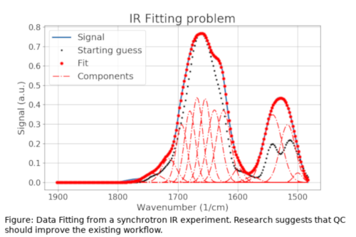
The advancement of quantum technologies is expected to pave the way for practical Quantum Computing (QC). Practical QC should provide solutions to certain problems, superior to those offered by the classical computational paradigm. The QC field is [in development][1] but has not taken its final form yet. In an attempt to define requirements for its practical use, this research reviews the current state of QC services as provided by IBM, Microsoft , Rigetti and D-Wave, and proposes potential applications in the synchrotron radiation facility Elettra Sincrotrone Trieste. This research has concentrated its focus on potential applications that may benefit from using QC for Optimization problems [1] even if it acknowledges other uses in fields like those of simulation modelling and information theory. In specific, this work starts by hinting on the optimisation needs for accelerator control till beamline end-station uses in scientific applications like X-ray Fluorescence data fitting [Fig.1] and Ptychography reconstructions. The connection of QC to specific practical optimisation problems in a synchrotron may serve as a partial guideline for the future development of the field.
Ultrafast, ultra-low noise X-ray detectors based on Avalanche PhotoDiodes (APDs) are crucial elements in scientific contexts such as Synchrotron Radiation facilities and Free Electron Lasers. APDs have been traditionally based on silicon, a mature and solid technology with adequate performance up to the X-ray range. However, the advent of ultimate light sources set more stringent requirements on APD detectors, which would benefit from a new choice of materials. In particular, in GaAs-based semiconductors the higher Z number of Ga and As compared to Si strongly increases quantum efficiency. Consequently, much thinner absorption regions are sufficient, resulting in improved time resolution. Furthermore, GaAs has a higher energy gap than silicon (thus a better resistance to radiation damage) and epitaxial growth of AlGaAs alloys allows exploiting quantum confinement effects through band gap engineering.
We are developing APDs with separated absorption and multiplication regions, where the latter is made of a staircase GaAs/AlGaAs multilayer, which favors well defined multiplication of electrons and suppresses multiplication of holes (lower noise of device). We will present details of the working principle and fabrication protocols, as well as of detector performance in terms of multiplication and noise, under radiation from the visible to the X-ray range.
The recently commissioned Extremely Brilliant Source (EBS) has substantially enhanced the nano probe capacities at the ESRF. Nano diffraction imaging has been boosted by these capacities to improve in spatial resolution reaching length scales relevant for a variety of materials that are candidates for quantum computing. As band structure properties in all semiconductors sensibly depend on lattice strain, a high-resolution tool like X-ray nano diffraction can reveal subtle local variations of strain with unique definition in terms of lattice parameter sensitivity. Strain landscapes of few 10-5 can be imaged, with spatial resolution reaching now the sub 50 nm regime. High-resolution imaging of strain fields and crystalline defects in 2D quantum wells and semiconductor nanowires show the potential of this new imaging technique available to the entire user community through the public ESRF user program.
Quantum materials exhibit unique physical phenomena, especially if grown in ultra-thin films or in heterostructures with other materials. We have built and operated a dedicated UHV facility where multiwavelength Pulsed Laser Deposition can synthesize quantum materials and directly deliver the atomic-layer controlled samples to an all-resolved photoemission apparatus (SP-ARPES) and to an end-station for XPS, XAS, XMCD that exploit the NFFA-APE sources on the Elettra synchrotron. Open access is granted via NFFA (www.NFFA.eu; www.Trieste.NFFa.eu). Along with users science we carry on in-house research and Ph.D. projects.
One example of relevance in quantum material science is the study of the electronic properties of anatase TiO2 thin films, e.g. the stabilization of in-gap states has been found to be correlated with the amount of Ti3+ ions by Resonant XPS and ARPES that also has provided evidence of the formation of a two-dimensional electron gas (2DEG). Both in-gap states and 2DEG are very sensitive to structural modification of thin films, such as substrate-induced strain, surface reconstruction, and thickness. Their formation and evolution were investigated down to the single-unit-cell and sub-unit-cell thickness thus indicating that no-critical thickness is required to stabilize the 2DEG at the anatase TiO2 surface and implying its purely 2D nature.
Implementing all-resolved photoelectron spectroscopy (ARPES, SpinPES, SPARPES) with temporal resolutions, in pump-probe mode, requires dedicated facilities capable to deliver ultrashort photon pulses (~100 fs) in the Extreme Ultraviolet (EUV) region with an adjustable repetition rate up to the MHz range to provide the necessary statistics while maintaining the photoexcitation density safely in the perturbative linear regime. We have built the NFFA-SPRINT versatile UHV twin-beamline setup for advanced photoemission experiments based on table-top laser HHG source operating in the EUV range (17-31 eV) with repetition rate up to 200 kHz. Two end stations provide ARPES spectrometers, Vectorial Spin Polarimeters and surface science facilities, including UHV transfer from PLD/MBE growth systems. The operational set-up, opened to international users in 2019, has proven to deliver monochromatic EUV pulses shorter than 100 fs and with energy resolution of 18 meV in experiments on transition metals and topological insulators. Thanks to the high repetition rate, these features are fully exploitable for space-charge free PES/ARPES experiments i.e. with space-charge broadening effects reduced below the energy resolution of the measurements.
The high tunability multi-OPA configuration allows the realization of the first pump/probe experiments on various materials, from nanoparticle to thin films, from ferromagnetic structures to semiconductors.
*https://www.trieste.nffa.eu/techniques/spectroscopy/time-resolved-pes-and-spin-polarization-sprint/
This contribution presents the femtosecond pump-probe laser infrastructure of the Soft X-ray Port (SXP) scientific instrument at the European XFEL. This experimental platform is primarily designed for time- and spin-resolved photo-electron spectroscopy, but investigations of complex chemical and bio-inorganic molecular systems by means of fluorescence spectroscopy as well as research on highly charged ions is also envisioned. It is located behind the SASE3 soft X-ray undulator providing FEL radiation with variable polarization in the photon energy range between 260eV and 3000eV (4.8nm to 0.4nm) with 0.1 to 2x10e14 photons per pulse and up to 27000 pulses per second. Two high-quality elliptical mirrors in Kirkpatrick-Baez configuration will focus the femtosecond FEL pulses to a FWHM spot size of approximately 1µm in diameter, resulting in an intensity of more than 10e18 W/cm2 in the interaction region. Together with a powerful synchronized laser amplifier system, whose wavelength range is currently extended into the infrared as well as extreme ultraviolet region, it will pave the way for ultrafast pump-probe investigations at the SXP instrument combining intense and tunable soft X-rays with versatile optical laser capabilities.
The effect of pulse wavefront (WF) distortion ranges from change in the radiation deposition mechanism, to inability to reach diffraction limited foci, and limitations in spectral correlations between spectrometers. The effect goes well beyond 'bad quality' beam and may determine the capability and the scientific goal of the experiment altogether. At the same time, the technique used to resolve such WF distortion in high resolution is equally an excellent tool in monitoring the changes in the sample internal features. At European XFEL several studies are proceeding in parallel to handle the issue. Here are some of the visual and experimental confirmation of the effect of WF distortions under various contributors, its detection methods and the impact on experimental results for near-distortion-free pulses.
Quantum materials nowadays hold the key to develop new technologies that satisfy the increasing societal demands in terms of communication and data handling while being sustainable and ecofriendly. The technological development relies on the ultimate understanding of the materials properties as well as on the definition of new pathways to control their properties. Femtosecond time-resolved photoelectron spectroscopy (TR-XPES) with laser sources has proven to be a powerful tool to the understanding and coherent control of quantum materials. However, the accessible photon energies, limited to around 100eV, prevent the full exploitation of this technique. Experiments at higher photon energies with femtosecond time resolution are only possible at MHz free electron lasers due to space charge effects. In this contribution, we present the SXP instrument at the European XFEL conceived as an open port with various interaction points, one of which hosting a TR-XPES setup with a momentum microscope. The photon energy range available at the SASE3 undulator, 0.25keV to 3keV, and the variable polarization will allow the simultaneous characterization of the electronic, magnetic and structural properties of quantum materials. A wide range of laser wavelengths, from the XUV to the THz region, will be available to study dynamics and quantum control.
Training is becoming an increasingly important topic to facilitate the work of scientists at accelerator-based photon sources and also to introduce young scientists to specific areas such as modern quantum technologies. One of the goals of ExPaNDS (European Open Science Cloud (EOSC) Photon and Neutron Data Service) is to train research scientists in order to better understand the issues, methods and available computational RI infrastructures to address critical research questions.
The ambitious ExPaNDS project itself is a collaboration between 10 national Photon and Neutron Research Infrastructures (PaN RIs). The project aims to deliver standardised, interoperable, and integrated data sources and data analysis services for Photon and Neutron facilities.
Our PaN-training catalogue, providing a one-stop shop for trainers and trainees to discover online information and content, including training materials, events and interactive tutorials. the catalogue provides opportunities to promote training events and news, and to contribute to a growing catalogue of materials; for trainers, the portal offers an environment for sharing materials and event information; for trainees, it offers a convenient gateway via which to identify relevant training events and resources, and to perform specific, guided analysis tasks via customised training workflows to provide FAIR research.
In the last decades, advances in the generation and manipulation of ultrashort light pulses allowed photon and electron spectroscopies to access the time domain in the consolidated pump-probe scheme. Refined in several aspects, the technique has demonstrated its versatility in accessing the dynamics and transient states produced by impulsive photoexcitation on various physical systems, opening new perspectives for light-induced phase transformations. In this scenario, we propose a multi-messenger spectroscopic approach where the absorbed/scattered photons, photoemitted electrons, and electron-spins are measured as messengers of energy, momentum, and spin of the out-of-equilibrium states after coherent ultrafast photoexcitation of the system.
At the SPRINT-NFFA facility, we developed a time-resolved optical and Raman spectrometer for pump-probe experiments with sub-ps time resolution on samples spanning the 8-350 K range under UHV conditions. The laser system, comprising multiple-OPA and a table-top HHG source, can deliver, in a two/three-pulse scheme, ultrashort (⁓100 fs) IR-to-XUV pump pulses and visible sub-ps probe pulses for Raman and optical measurements. The reflected/scattered signal is collected at variable angles. The UHV chamber is coupled, via UHV-suitcase, with the angle- and spin-resolved photoelectron spectroscopy setups already operative at the facility*. We will present the experimental setup layout discussing the first experimental test results.
TUTORIAL
Soft-X-ray angle-resolved photoelectron spectroscopy (ARPES) in the photon-energy range around 1 keV combines resolution in electron momentum k with enhanced photoelectron escape depth. These benefits allow previously unthinkable k-resolved electronic structure studies on buried heterostructures and impurities, which are in the heart of solid-state quantum devices.
For example, soft-X-ray ARPES experiments on AlGaN/GaN high-electron-mobility transistor heterostructures find anisotropy of the interfacial quantum-well states, resulting in anisotropic high-field electron transport [Nature Comm. 9 (2018) 2653]. For the oxide interfaces LaAlO3/SrTiO3, resonant photoexcitation of the Ti-derived interfacial charge carriers resolves their multiphonon polaronic nature, fundamentally limiting their mobility [Nature Comm. 7 (2016) 10386]. Experiments on NbN/GaN superconductor/semiconductor heterostructures find that the Fermi states of NbN are well separated from the GaN states in energy and k. Excluding poisoning of the superconductivity, this allows the integration of NbN-based quantum devices into semiconductor technology [Sci. Adv. 7 (2021) eabi5833].
Impurity systems are illustrated by In(Fe)As, where resonant photoexcitation of the Fe-derived states identifies their full integration into the conduction band of GaAs, allowing high mobility of spin-polarized electrons [Phys. Rev. B 103 (2021) 115111]. Other cases include magnetic V impurities in the topological Bi3Se2 competing with the quantum anomalous-Hall effect, etc.
Quantum electronic devices in epitaxial semiconductor heterostructures are based on an extremely precise level of control of the control of structure and compositions. Epitaxial growth techniques provide substrates with exceptionally low concentrations of chemical impurities and structural defects such as dislocations and stacking faults. The advent of quantum devices establishes a new range of structural problems associated with the comparatively large size of quantum devices and the small splitting of quantum states. Structural features of interest include atomic steps at heterostructure interfaces, complex stress distributions arising from the formation of electrodes, and the thermal stress arising during cooling to low temperatures. This talk surveys the electronic evidence for structural effects and illustrates the scale of distortion relevant to quantum devices. Prospects for exploiting these structural features to provide new routes for device fabrication will be presented. Other structural effects will impact the integration of other quantum devices and will be briefly discussed.
In materials with inhomogeneity, macroscopic properties depend not only on local electronic or magnetic properties but also on the way inhomogeneity is spatially distributed. Controlling this spatial pattern may therefore create new functionality. Modern X-ray sources provide the means for mapping out the spatial distribution of, e.g., magnetic domains or coexisting phases as well as for tracking the evolution of spatial patterns in time. Such experiments enable us to develop strategies for controlling disorder. I will show examples for coexisting phases and complex magnetic patterns and will discuss relevant length and time scales for future experiments.
Understanding the relationship between entangled degrees of freedom (DOF) is a central problem in correlated quantum materials and the possibility to influence their balance is promising toward realizing novel functionalities. In the single-layer iridate Sr2IrO4, the interaction between spin–orbit coupling and electron correlations induces an exotic ground state with magnetotransport properties promising for antiferromagnetic spintronics applications. Moreover, the coupling between orbital and spin DOF renders the magnetic structure sensitive to the Ir–O bond environment. We use strain engineering to perturb the local lattice environment and, by tracking the response of the low-energy elementary excitations by Resonant Inelastic X-Ray Scattering (RIXS), we unveil the response of the microscopic spin and charge interactions. By applying tensile strain, we observe a large softening of the spin(-orbital) wave dispersion along the [h,0] direction and a simultaneous hardening along the [h,h] direction. This evolution entails a strain-driven crossover from anisotropic to isotropic interactions between the magnetic moments. We also show how the charge excitations are coupled to the lattice in Sr2IrO4. We unveil the evolution of a dispersive electron-hole pair excitonic mode which shifts to lower (higher) energies upon compressive (tensile) strain, manifesting a reduction (increase) in the size of the charge gap.1
The interplay between spin-orbit interaction (SOI) and magnetic order is currently one of the most active research fields in condensed matter physics. We report on ferrimagnetic switching driven by stochastic resonance in multiferroic (Ge,Mn)Te, investigated by x ray magnetic linear and circular dichroism (XMLD/XMCD), supported by SPR-KKR-CPA scattering and magnetic cluster calculations. In accordance with our previous resonant ARPES results, we find that the Mn-atoms occupy two distinct substitutional and interstitial lattice sites by substituting Ge-atoms. We show that (Ge,Mn)Te antiferromagnetically couples its Mn-sites with slightly different magnetic moments, resulting in a ferrimagnetic order. One of the astonishing results is that XMCD data show that the system spontaneously switches its magnetisation direction, without changing external parameters such as light helicity, applied B-fields or temperature (up to 65 K). The switching reveals ultra-slow magnetization dynamics, which can be governed by the stochastic resonance. Finally, we demonstrate that the occurrence of ferrimagnetic switching is closely related to the formation of topological spin textures in the films, enabled by the interplay of antiferromagnetic and Dzyaloshinskii-Moriya interactions.
The statistical features of the radiation emitted by Free-Electron
Lasers (FELs), either by Self-Amplified Spontaneous Emission
(SASE-FELs) or by seeded emission (seeded-FELs), are attracting
increasing attention because of the use of such light in probing high
energy states of matter and their dynamics. We decided to shift the focus from correlation functions towards the reconstruction of the distribution
of the occupation numbers of the radiation energy states.
We propose a Maximum Likelihood reconstruction of the diagonal elements
of the FEL radiation states based on the statistics of no-click events.
The ultimate purpose of such a novel
approach to FEL radiation statistics is the experimental confirmation
of the departure from Poissonian statistics that SASE-FEL radiation exhibits and the laser-like coherence of seeded-FEL light. In this framework, it is interesting to note that the outcome of this work can be extended to any process of harmonic generation from a coherent light pulse, ushering in the study of the preservation or generation of quantum features in general non-linear optical processes.
Quantum imaging methods, analogous to ptychography, have been recently proposed to assess the state of quantum systems. In ptychography, an overlapping illumination scans a sample and generates diffraction patterns that can be numerically converted to a high-resolution image of the sample. An ideal conversion demands precise knowledge of scan coordinates, low-noise measurements and illumination stability. In practice, the aforementioned criteria might not be completely achievable. Thus, the computational conversion inevitably fails to converge. We demonstrate an automatic differentiation based ptychography that optimises fluctuations leading to successful imaging for photon sources exhibiting shot-to-shot fluctuations, like X-ray free-electron lasers. Automatic differentiation is used in deep learning and optimisation as a set of techniques for evaluating derivatives. Various quantum imaging approaches can benefit from the proposed ptychography platform, like ghost imaging at soft X-ray free-electron lasers. We report on the results of our recent ptychography experiments at the FLASH2 facility at DESY.
Soft X-ray spectroscopies usually average the observed response of a sample across the entire illuminated area. This restricts the obtainable information, especially if the sample is inhomogeneous (either because of electronic domain formation or patterning on the micro- and nanoscale). Formation of electronically distinct domains has been observed for various quantum materials. A complete understanding thus necessitates a domain-resolved experimental approach.
We demonstrate the implementation of an experimental setup, build around an off-axis Fresnel zone plate, which enables imaging X-ray absorption spectroscopy and resonant inelastic X-ray scattering with a current spatial resolution down to 1.8µm. The zone plate, located between sample and detector, disperses X-rays scattered from the sample and also images the sample along the direction perpendicular to the dispersion. Incident X-rays are focused to a 1mm long line such that excitation spectra from each point along the line are measured in-parallel.
In a microstructured VO2 thin-film, we find that the structure edges undergo the insulator-metal transition earlier than the centers, hinting at facilitated strain release. We believe that the observed effects apply in general to patterned films of quantum materials and provide a tool for adequate experimental studies.
Reference: J.O. Schunck et al. Optica 8(2), 2021