Speaker
Description
Recent millimeter-wavelength telescopes require cryogenically cooled optics to achieve a high-sensitivity observation. A broadband anti-reflection (AR) technology that works at cryogenic temperature has been desired. Silicon is one of the suitable materials for millimeter-wave optics in cryogenic use. This is because it shows low-loss at a cryogenic temperature in the millimeter wavelength.
AR methods using sub-wavelength structures (SWS) have been reported. We designed the SWS on silicon that shows the averaged reflection of 2 % from 100 to 450 GHz. The structure that we designed consists of 4-layer discrete grid structures $^{[1]} $.
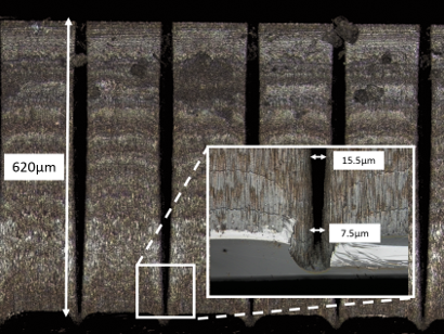
The most challenging part of the fabrication for the structures is to make the high-aspect-ratio trenches which have 13 $\mu $m width and 620 $\mu $m depth. To realize this, we employed a deep reactive ion etching (DRIE) process. This technique allows to make an anisotropic high-aspect-ratio structure. Using DRIE process, we succeeded to fabricate trenches which have required shape (Fig. 1).
We studied two methods to fabricate 4-layer structures. The first one is to adopt the DRIE process for fabrication of all the layers. The second one is to use a combination of the DRIE and the direct machining process with a dicing saw. We present the prototypes of the multi-layer SWS on silicon using these two different methods.

Reference
$^{[1]}$ T. Hasebe et al., “Concept study of optical configurations for high-frequency telescope for LiteBIRD,” J. Low Temp. Phys. 193, 5 (2018).
| Student (Ph.D., M.Sc. or B.Sc.) | N |
|---|---|
| Less than 5 years of experience since completion of Ph.D | Y |
