Choose timezone
Your profile timezone:
Low Temperature Detector Development and Physics
HOLMES is an experiment with the goal of performing a direct measurement of the neutrino mass from the electron capture spectrum of 163Ho. In order to reach its goal sensitivity of 2 eV it is necessary to gather as many as 10e13 events in the three years projected live time of the experiment. To do so, HOLMES will deploy an array of 1000 low temperature calorimeters composed by a Transition Edge Sensor (TES) thermometer coupled to a gold absorber, where 163Ho will be embedded, via a custom ion implanter. With a target activity of 300 Bq for each absorber, pile-up will be the main limiting factor in the sensitivity for the neutrino mass.
In order to keep the pile-up fraction at 1e-4 it is crucial to have signals with an exponential rising edge of ~10 us sampled at a proper rate (500 kHz) so that pile-up resolving algorithms may be applied. Besides, an energy resolution of the order of few eV is needed not to spoil the neutrino mass measurement.
In this contribution I will describe the detectors used in HOLMES, their performance and the RF-SQUID based multiplexed readout system which will allow us to simultaneously operate 1000 detectors at 100 mK and collect the necessary data to reach the 2 eV target sensitivity of the neutrino mass.
The Advanced Telescope for High ENergy Astrophysics (ATHENA) will include the X-ray Integral Field Unit instrument (X-IFU). This instrument is baselined with an array of 3,168 transition-edge sensor (TES) pixels made with Mo/Au bilayers that will be AC biased and Frequency-Division Mutliplexed (FDM). Over the last few years, there has been intense effort at NASA/GSFC and SRON to better understand and optimize the pixel design to meet the requirements of X-IFU. This has included investigation of the effect of TES design on transition shape and uniformity, noise, eddy-current losses, AC Josephson effects, and spectral resolution over a broad range of incident energy. Through this understanding we have been able to achieve ground-breaking performance under AC bias. In this presentation, we will discuss the important physical effects in the TES, and describe how they are driving the choice of TES parameters (size, aspect ratio, thermal conductance, resistance, heat capacity etc.) that are being considered for X-IFU. We will also discuss the latest measurements of NASA TES devices and how they are further improving our understanding of the relevant physics in the TES. This will include our advances in modeling the TES as multiple thermal bodies, and how the design of X-ray absorber attachments may influence TES performance.
At SRON Netherlands Institute for Space Research, we are developing X-ray microcalorimeters as backup option for the baseline detectors in the X-IFU instrument on board of the ATHENA space mission led by ESA and to be launched in the early 2030s.
New, mixed 5X5 TiAu Transition Edge Sensor (TES) arrays where TESs have different high aspect ratios and high resistance have been fabricated to meet the requirement of the X-IFU instruments. Such arrays can also be used to optimize the performances of the Frequency Domain Multiplexing (FDM) readout and eventually can lead to large detector arrays.
In this work we present the results obtained on tens of devices with an aspect ratio ranging from 1-to-1 up to 1-to-5 measured in the single pixel mode, with the FDM readout developed at SRON/VTT. We observed an nominal energy resolution of about 2.5 eV at 5.9 keV and at bias frequencies from 1 to 5 MHz. The measurements have been done in the high inductance limit regime, implying that we are still far from their intrinsic energy resolutions. Thermal and electrical parameters have been compared by means of AC complex impedance and noise spectra measurements to have a clear picture of the performances of these arrays.
These detectors are proving to be the best TES microcalorimeters ever reported in Europe, being able to accomplish not only the specifications of the X-IFU instrument, but also those ones for other future challenging X-ray space missions, fundamental physics experiments, plasma characterization and material analysis.
We are now ready to test the uniform kilo pixels array in combination with the FDM readout in multi pixels mode.
Acknowledgment
This work is partly funded by European Space Agency (ESA) under ESA CTP contract ITT AO/1-7947/14/NL/BW, and is partly by the European Union’s Horizon 2020 Programme under the AHEAD project with grant agreement number 654215.
Low Temperature Detector Development and Physics
Intense development of nanobolometers has taken place for well more than a decade with the aim to reach noise equivalent power NEP = 10e-20 W/rtHz. Furthermore, observation of single photons at increasingly long wavelengths is a long-standing effort. We present a microwave nanobolometer based on superconductor/normal-metal/superconductor Josephson junctions. Using positive electrothermal feedback, we show that we can achieve a single-shot detection ?fidelity of 0.56 for 1.1-zJ pulses of 8.4-GHz photons [1]. This is more than an order of magnitude improvement over the previous thermal detectors. Furthermore, we observe that we can reach NEP = 2*10e-20 W/rtHz with our detector in the linear bolometric mode [2]. The measured frequency dependence of the NEP suggest that this bolometer is capable of detecting single 0.3-zJ photons. These results were achieved by integrating the bolometer with a quantum-limited Josephson parameteric apmli?er and further improvements are expected for example using two-dimensional materials.
[1] J. Govenius, R. E. Lake, K. Y. Tan, and M. Möttönen, Phys. Rev. Lett. 117, 030802 (2016).
[2] R. Kokkoniemi et al., arXiv:1806.09397 (2018).
Future space-based observatories for the far infrared and sub-mm wave radiation, such as SPICA and the OST telescope, will need ultra-sensitive background limited detectors at frequencies above 1THz. We develop a KID that combines photon noise limited performance, high optical efficiency, broad band and dual polarization radiation coupling operating between 1.4 and 2.8THz, with a NEP below 3x10$^{-19}$W/Hz$^{1/2}$, and good agreement between the measured and expected optical efficiency. The fractional power ratio between the powers received by the dual polarized detector and by the single polarized counterpart is a factor 2.
The detector consists of a hybrid NbTiN/Al Kinetic Inductance Detector, fabricated on a Si substrate. Radiation coupling is achieved using a leaky lens antenna fabricated on a suspended SiN membrane. The radiation is coupled to the leaky lens antenna using a Si lens placed on top of it at a distance of 6μm. The absorbing section of the KID is fabricated entirely from Al, and integrated with the antenna to absorb power from both polarizations directly in the KID. The device shows photon noise limited performance with a NEP below 3x10$^{-19}$W/Hz$^{1/2}$ around 1.55THz with the expected optical efficiency. The dual polarized device receives twice as much power from an incoherent source than the single polarized one. Additionally, we measure the antenna beam pattern at the same frequency band and find a good match between the measured and simulated beams in reception. Standard transmission simulations are not fully correct due of the intrinsic multi-moded nature of the antenna. To verify the frequency coverage, we measure the frequency response using a Michelson interferometer to find broad band coupling in matching our simulations.
The presented design is upgradable to frequencies up to 10THz using e-beam lithography. These results indicate that broad band, dual polarization radiation coupling above 1THz is feasible using antenna coupled KIDs.
After more than 15 years of development, the technical maturity of MKIDs has greatly improved. Array level demonstrations of imagers and spectrometers now exist, measuring a wide coverage of frequencies, and with multiple optical coupling schemes. However, several different technical challenges must be overcome before MKIDs reach the point where they become a general solution for the full suite of astronomical and instrumental applications. First, MKIDs have not consistently shown background limited sensitivity, especially at the low frequencies (< 1 Hz) essential to bolometric observations. Also, modern bolometric cameras require use of advanced focal planes in which the detectors are comprised of integrated circuits performing multiple functions such as optical coupling, diplexing, and on-chip filtering of multiple frequency bands within 1 spatial pixel.
Our efforts at NIST have been to both extend the successful direct-absorber style polarimeters pioneered for use in the balloon-borne instrument BLAST and in production for TolTEC, as well as integrate MKIDs into the proven mm-wave circuitry of NIST’s well-established OMT-coupled TES bolometer arrays that have been delivered to many collaborations. We have extended the direct-absorbing MKID technology to longer wavelengths and lower photon loadings by creating hybrid MKIDs combining the low capacitive loss of the TiN-Si interface with the high sensitivity and lower sheet resistance of thin Al inductors. We also prevent the well-known aging of the Al through the deposition of a thin passivation layer without compromising their performance. These sensors show photon limited performance well below 1 Hz. Furthermore, we have also integrated Al-based inductors and amorphous-Si based parallel-plate capacitors into an OMT-coupled circuit and have initial results of photon-noise limited performance.
In this talk, I will present how we combine spectroscopy and imaging capabilities inside one compact device for submillimeter observations. This system is an interferometric system that has been designed to fulfill the spectroscopic requirements of a space mission. The idea is to bring a Fabry-Pérot spectrometer very close to the detector (silicon bolometers) such that they form a coupled, resonant system with enhanced detection efficiency. For this purpose, we introduce a new type of Fabry Pérot for submillimeter spectroscopy: instead of having metal mesh mirrors, we use an assembly of thin silicon sheets. Theoretical simulations have shown that the use of dielectrics instead of metals suppresses the ohmic losses thus leading to increasing the absolute efficiency of the spectrometer. In order to reach a high finesse similar to what we have in the case of interferometers made with metallic grids, we choose to assemble several silicon sheets to form one mirror as defined by the Bragg mirror theory. Moreover, we have found that the coupling of the spectrometer with the detector is close to perfect: the absorption of the whole assembly has almost 100% efficiency for wavelengths corresponding to the size of the resonant cavity of the Fabry Pérot. This system may lead to a real improvement and can reduce the observations time by a factor of 2, which is not negligible at all. In the second part of the talk, I will describe how we have built the mirrors and what optical tests we have performed to conclude that the silicon sheets are perfectly compatible with the finesse of our spectrometer. Finally, I will present the last measurements that we did with the silicon spectrometer at cold temperature (4K).
Arrays of lumped-element kinetic inductance detectors (LEKIDs) optically coupled through an antenna and transmission-line structure are a promising candidate for future cosmic microwave background (CMB) experiments. Using the separated architecture of a LEKID enables optical coupling to be realised, without the detector becoming susceptible to two-level system noise created by the amorphous-dielectric requirements of a simple microstrip feedline structure. Through initial investigations of small prototype arrays, we have shown this compact device architecture can produce intrinsic quality factors > 10$^5$, allowing for MUX ratios to exceed 10$^3$. Moreover, we have demonstrated that these devices are limited by generation-recombination or photon noise down to low modulation frequencies proving the devices are not susceptible to the fabrication requirements of any antenna feed or filtering network the device is coupled to. However, this optical configuration is highly susceptible to a reduction in sensitivity due to stray light. Here we discuss our investigation into a suitable method of stray-light suppression based on the addition of an absorbing layer compatible with our device design and present the current performance of our prototype devices.
Low Temperature Detector Development and Physics
Microwave Kinetic Inductance Detectors (MKIDs) were invented in 1999 at
Caltech and JPL with the promise of both high detector sensitivity and
an easy solution to scale into large arrays. Over 20 years of
significant development, MKIDs have fulfilled this promise with their
sensitivity approaching the fundamental limit and the pixel count
reaching 10^5. The technical maturity of MKIDs have brought them broad
applications in astronomical instruments from mm-wave, IR/visible to
X-ray for ground-based, sub-orbital and space missions, as well as
non-astronomical applications such as dark matter search and quantum
information science. In this talk, I will review the technical progress
in the understanding of device physics, the techniques invented for
improving the sensitivity, the implementation of various optical
coupling schemes, the study of materials, and the development of
fabrication process for large arrays, made over the past 20 years.
I describe the design, principle of operation and results from our X-ray TKID prototype arrays. These superconducting pair-breaking detectors exploit the ease with which MKIDs can be frequency-domain multiplexed to create large arrays of X-ray microcalorimeters with absorbers that can be close-packed and tiled. Arrays of 20,000+ TKIDs are potentially achievable using frequency domain multiplexing electronics that are similar to those already used to read out 20,000+ pixel MKIDs optical arrays. Sensitivity is controlled by placing absorbers with tuned heat capacity on thermally isolated membranes and by use of low T$_c$ superconductors. Noise, from two-level systems and the readout, is minimized by control of the MKID geometry and use of very low noise amplifiers. Quantum efficiency is tuned by selection of X-ray absorber materials and thicknesses, just as for TES X-ray microcalorimeters. While the energy resolution of past devices is 75 eV at 5.9 keV, we report on progress to achieve 10 eV resolution in forthcoming design iterations. Results include the quiescent performance of individual TKID resonators and initial X-ray pulse data.
To answer the question whether there is life on exoplanets a new generation of instruments is required that will take spectra of these planets. Future instruments for visible/near-IR wavelengths therefore require noiseless, photon counting detectors, with energy resolution.
Microwave Kinetic Inductance Detectors (MKIDs) are photon-counting superconducting detectors which provide energy resolution in each pixel. The resolving power (R=E/dE) of MKIDs is theoretically limited to R~100 by Fano statistics, depending on the material. Current detectors reach R~10, thus we need to better understand the physics and improve the detector limits.
We present an energy resolution study with aluminium MKIDs, which we have previously shown to understand very well and which are the most sensitive terahertz MKIDs to date. We deliberately study a well-understood material first, before moving to higher resistivity materials, which are favourable from a photon-absorption standpoint. We have measured the resolving power of Al MKIDs, which from their THz sensitivity promise R~60 at 400 nm. We operate the MKIDs at 120 mK and illuminate them with 4 lasers between 402-1550 nm. Firstly, we find that our BK7 and fused silica windows are open to low frequency stray light (< 1 THz), which limits the measured energy resolution. After mounting the optical fiber at 100mK, we show that we reach a resolving power of 17 at 402 nm to 10 at 1550 nm from the histogram of single-photon events, with a large (factor ~4) discrepancy between the signal-to-noise and the histogram resolution. We expect that the loss of hot phonons, while down converting the photon energy to quasiparticles, is already showing up at this energy-resolution level. Al MKIDs are particularly sensitive to phonon losses because of the long pair-breaking time. We will present experiments to study the effectiveness of phonon trapping measures.
The kinetic inductance detector (KID) offers an elegant and convenient solution to building large-format arrays operating at mm-wavelengths. Scaling alternative technology to the large detector counts required for future experiments requires auxiliary multiplexing components that can significantly increase the complexity and cost. Arrays of KIDs require no additional cryogenic multiplexing hardware, only needing a single commercially available low-noise amplifier. A number of experiments are set to serve as the first major demonstrations of KID technology. Of these, the KID design is based on direct free-space absorbing lumped-element KIDs. While effective for single-colour observations, these designs are not directly compatible with the multi-colour on-chip transmission line filtering techniques that have been shown to offer improved focal plane efficiency for wide-band imaging applications. In this presentation we will discuss the recent developments and performance of the antenna-coupled lumped-element KID; a simple KID implementation that permits efficient radiation coupling through a mm-wave microstrip feed. We discuss progress on the design and characterisation of our first prototype lens-coupled twin-slot antenna arrays. We will present results from recent lab-based full optical characterisation and discuss improvements for subsequent design iterations. We will also present preliminary designs and performance of a horn-coupled variant that offers wider bandwidth, reduced parasitic loading, and improved beam systematics. We will present results of initial measurements, and details of our current efforts toward scaling to a full wafer-scale demonstration array operating at 280 GHz.
Technology transfer, outreach, and dissemination
Real-time video rate imaging and automatic recognition of threats and contraband items that were concealed beneath layers of clothing on moving passengers was recently demonstrated with a prototype passive sub-mm imaging system at Cardiff Airport in the UK. The passengers did not have to divest their outer clothing layers and the instrument was able to distinguish between threat and non-threat items with excellent accuracy in less than the amount of time it takes to pass across the field of view. This level of performance for a passive imaging system is only achievable with low temperature detector systems and, although the financial cost of such systems may be high relative to currently available technology, this is easily offset by the associated benefits; such as increased passenger throughput, reduction of required real estate, avoidance of electromagnetic radiation exposure and, of course, an overall improvement in the passenger experience. Our prototype security imaging system is based on arrays of Aluminium LEKIDs operating at 250mK in a cryogen free cooling platform with compact scanning optics, narrow band optical filters, fast signal processing electronics and a machine learning application for threat detection that was trained with many thousands of marked-up images. We look forward to presenting the latest results of our development.
We report on the development of commercially fabricated multi-chroic antenna coupled Transition Edge Sensor (TES) bolometer arrays for Cosmic Microwave Background (CMB) polarimetry experiments. The orders of magnitude increase in detector count for next generation CMB experiments require a new approach in detector wafer production to increase fabrication throughput.
We describe collaborative efforts with a commercial superconductor electronics fabrication facility (SeeQC-HYPRES, Inc.) to fabricate antenna coupled TES bolometer detectors. We have successfully fabricated an operational dual-polarization, dichroic sinuous antenna-coupled TES detector array on a 150 mm diameter wafers. The fabricated detector array has yields of over 96% and excellent uniformity across the wafer. We have also demonstrated stable detector performance over 4 months. Both RF characteristics and TES bolometer properties are suitable for CMB observations. We successfully fabricated different types of TES bolometers optimized for frequency-multiplexing readout, time-domain multiplexing readout, and microwave SQUID multiplexing readout. We discuss the motivation, design considerations, fabrication processes, test results, and how industrial detector fabrication could be a path to fabricate hundreds of detector wafers for future CMB polarimetry experiments.
Low Temperature Detector Applications
The dark matter problem has accompanied cosmologist and particle physicist for more than 80 years. Nowadays we have an extremely accurate model of our Universe, but still most of its content eludes our observation. Grasping the nature of this missing matter is of compelling necessity for our understanding. Direct searches aim to detect dark matter particles with Earth-bound detectors. Low-temperature detectors play a crucial role in this challenging hunt, with their capability of accessing interactions of light dark matter particles well below the WIMP-scale. A review of the most sensitive cryogenic approaches to dark matter search and of recent results will be given together with a glance on future prospects.
We have designed and tested a large area 11-gram photon detector with 45 cm$^2$ surface area and 3.9 eV energy resolution, employing a TES-based readout on a Si absorber. With a 20 $\mu$s rise time due to the fast collection of athermal phonons, this device significantly surpasses both timing and energy resolution requirements of future neutrinoless double beta decay experiments.
Though not optimized for dark matter searches, this device was operated in collaboration with SuperCDMS in a short exposure light-mass DM search on the surface for 10 gram-days. The results of this search illustrate both the immediate and long term scientific potential of athermal phonon sensor technology for light mass dark matter direct detection.
The EDELWEISS collaboration is performing direct searches for light Dark Matter particles using cryogenic germanium detectors equipped with a charge and thermal signal readout. This versatile and highly performing technology opens new possibilities for searches for signals in the subGeV region, involving either electrons or nuclear recoils. This is attested to by results on Axion-Like Particles in the keV range, and by the attainment of the first sub-GeV spin-independent dark matter limit based on a germanium target. The search has been extended to Strongly Interacting Particles (SIMP) down to 45 MeV by exploiting the Migdal effect. New results on SIMPs with spin-dependent interactions will also be presented. Future developments will be discussed.
CRESST (Cryogenic Rare Events Search with Superconducting Thermometers) is a long-standing experiment with cryogenic detectors located at the underground facility Laboratori Nazionali del Gran Sasso in Italy. CRESST-III, the third CRESST experiment generation, is designed to probe the spin-independent Dark Matter(DM)-nucleus cross-section with a world leading sensitivity for low DM particle mass (less than 2GeV/c$^{2}$).
Despite many well motivated theoretical models for light dark matter, a large part of the parameter space for spin-independent scattering off nuclei remains untested for dark matter particles with masses below few GeV/c$^{2}$. CRESST experimental approach is the direct detection, which looks for scattering off nuclei of hypothetical dark matter particles inside a target of ordinary matter.
The CRESST-III experiment adopted scintillating CaWO$_{4}$ crystals of $\sim$25~g as target material for dark matter interactions. Each detector module is constituted by a CaWO$_{4}$ crystal paired with a plate made of Silicon-On-Sapphire for the detection of the scintillation light. Both crystals are equipped with Transition Edge Sensors (TES) and operated as cryogenic calorimeters at a temperature of $\sim$10~mK. The double channel read-out of scintillation light and total energy deposition is foreseen for event-by-event particle identification, a crucial feature for background suppression. In addition, a fully scintillating instrumented holder allows for identification of background events originated on the surrounding surfaces.
CRESST-III Phase 1 was successfully completed in 2018, achieving an unprecedented energy threshold for nuclear recoils. This result extended the present sensitivity to DM particles as light as $\sim$160~MeV/c$^{2}$.
In this contribution, a complete overview of the CRESST-III detectors will be presented, emphasizing the latest DM results and the perspectives of future stages of the CRESST experiment.
This talk will give an overview of the cryogenic detector for the most sensitive experiment to probe the QCD axion to date, Axion Dark Matter eXperiment, (ADMX). The detector technology includes a dilution refrigerator operated at 90mK and quantum-noise-limited amplifiers which contribute minimally to the system noise temperature thereby increasing the experimental sensitivity to the QCD axion. Using these technologies, ADMX has demonstrated recent success in reaching the so-called (DFSZ) sensitivity covering axion mass ranges from 2.66 to 3.31 μeV which no other axion experiment has achieved to this date. These results have crucial implications for the future direction of ongoing dark matter searches.
Detector readout, signal processing, and related technologies
Time-division multiplexing (TDM) is the most mature readout technology for transition-edge sensor (TES) microcalorimeter arrays. Our TDM architecture is routinely deployed to read out 250-pixel scale TES X-ray spectrometer arrays at synchrotron and accelerator beamlines, in table top X-ray spectroscopy experiments, and at electron beam ion trap (EBIT) facilities in applications ranging from materials science to nuclear physics. We continue to develop TDM to offer expanded capabilities in these applications and as a backup TES readout technology for the 3,168-pixel X-IFU instrument on the Athena satellite mission.
We will present results from a proxy 40-row TDM demonstration using NASA TESs that are within the design envelope under consideration for X-IFU. Since our existing 250-pixel TDM readout systems only have wiring to support 32 physically distinct TDM rows, the experiment read out 32 distinct TDM rows plus eight repeat rows for a total of 40 TDM timing rows, simulating the timing and noise of the true 40-row readout planned for X-IFU. Single-column measurements have a best-fit energy resolution of (1.91 ± 0.01) eV for Al Kα (1.5 keV), (2.10 ± 0.02) eV for Ti Kα (4.5 keV), (2.23 ± 0.02) eV for Mn Kα (5.9 keV), (2.40 ± 0.02) eV for Co Kα (6.9 keV), and (3.44 ± 0.04) eV for Br Kα (11.9 keV). Three-column measurements have a best fit energy resolution of (2.03 ± 0.01) eV for Ti Kα and (2.40 ± 0.01) eV for Co Kα. The demonstrated performance meets the dynamic range, energy-resolution, and crosstalk requirements of X-IFU. Larger scale true 40-row readout demonstrations will be conducted with a kilopixel scale TDM readout system that will come online in 2019.
We also report significant progress reducing crosstalk, with the goal of enhancing TDM performance in applications requiring tens or hundreds of X-ray counts per second per pixel. We will describe recent modifications to our cryostat wiring and SQUID multiplexer chips as well as performance in this regime.
Today microwave SQUID multiplexing appears to be the most suitable cryogenic multiplexing technique for reading out large-scale detector arrays based on metallic magnetic calorimeters. Here, each detector is read out by a non-hysteretic, unshunted rf-SQUID that is inductively coupled to a superconducting microwave resonator with unique resonance frequency. Due to the magnetic flux dependence of the effective SQUID inductance as well as the mutual interaction between the SQUID and the associated microwave resonator, the detector signal is transduced into a resonance frequency shift of the related microwave resonator which can be measured by standard homodyne or heterodyne detection techniques.
In this contribution, we report on our progress in developing a microwave SQUID multiplexer with 400 channels that is optimized for reading out metallic magnetic calorimeters and that provides a bandwidth of 1 MHz for each detector channel. It covers the frequency range from 4 GHz to 8 GHz which is set by the cryogenic low-noise HEMT amplifier that is used for boosting the multiplexer output signal. Compared to our previous multiplexer version, our latest generation is based on a different type of superconducting microwave resonators which allows for a significantly higher packing density. Moreover, the rf-SQUID is optimized with respect to the magnetic coupling between the SQUID and its input coil to overall enhance the energy resolution of the multiplexer as well as with respect to parasitic couplings, e.g. between the input and the modulation coil used for flux ramp modulation. Furthermore, we discuss the readout power dependence of the shape of the resonance curves, the peak-to-peak frequency shift as well as the overall noise performance of a microwave SQUID multiplexer. Finally, we present an advanced multiplexer model that is able to predict the observed power dependence.
We are developing the frequency domain multiplexing (FDM) read-out of transition-edge sensor (TES) microcalorimeters for the X-ray Integral Field Unit (X-IFU) instrument on board of the future European X-Ray observatory Athena. The X-IFU instrument consists of an array of $\sim$3000 TESs with a high quantum efficiency (>90 % at 7 keV) and spectral resolution $\Delta E$=2.5 eV @ 7 keV ($E/\Delta E\sim$2800).
FDM is the baseline readout system for the X-IFU instrument. In FDM, TESs are coupled to a passive LC filter and biased with alternating current (AC bias) at MHz frequencies. Each resonator should be separated beyond their detector thermal response (< 10 kHz) to avoid crosstalk between neighboring resonators. To satisfy the requirement of the X-IFU, a multiplexing factor of 40 pixels/channel in a frequency range from 1 to 5 MHz required.
Using high-quality factor LC filters and room temperature electronics developed at SRON and low-noise two-stage SQUID amplifiers provided by VTT, we have recently demonstrated good performance with the FDM readout of Mo/Au TES calorimeters with Au/Bi absorbers. We have achieved a performance requested for the demonstration model (DM) with the single pixel AC bias mode. We have also demonstrated 14-pixel multiplexing with an average energy resolution of 3.3 eV, which is currently limited by non-fundamental issues related to FDM readout in our current lab setup.
In this paper we report on the concept of the focal plane assembly, their requirements, detector performance under FDM scheme, recent results from pre-demonstration model setup and future prospect.
Low Temperature Detector Development and Physics
Superconducting nanowires have demonstrated remarkable performance in terms of efficiency, jitter, dark counts, and reset time. As a result, they have found application in fields ranging from deep-space communications to quantum communications. And recent discoveries have shown remarkable advances in the important performance parameters. However, a number of key developments remain either not fully understood, or remain to be applied to real-world uses. Among them, the development of large-area arrays for use in spectroscopy and imaging, and the development of sensitivity across a wider range of optical bandwidth.
In this talk, I will review recent developments in the field, focussing in particular on the interesting new role that the device microwave environment plays in device performance. I will also present some opportunities for integration of superconducting electronics with the nanowires. Finally, I will comment on opportunities for future work.
Superconducting Nanostrip Single-Photon Detectors (SNSPDs) are promising devices in many fields ranging from single-photon source characterization to optical communication and quantum cryptography. An important feature of SNSPDs is their low dark count rate (DCR), that increases close to the critical current where the detection efficiency is higher. In such a region DCR is dominated by a spontaneous resistive-state formation. The investigation of the origin of DCR toward optimization of SNSPD performances is crucial. Phase slip switching events have been considered recently as possible sources of dark counts in SNSPDs: a phase slip event is any process leading to a quantized phase change of the order parameter by 2p able to produce a finite voltage across the strip. Phase slip events include single vortices crossing an edge barrier and vortex-antivortex pairs splitting under the action of the Lorentz force driven by the bias current. In this work, we investigate phase slip events in 2D-NbN and NbTiN nanostripes, e,g, 5 nm thick and 80 nm wide. These materials are of great interest and widely used in SNSPD applications where very low dark count rates are requested. We measure the switching current distributions in a wide interval of temperatures from 6 K down to 0.3 K. The standard deviations of the switching distributions show an extended region at high temperatures where Multiple Phase Slip (MPS) switching events occur. This is probably related to a decreasing of the switching current and an increasing of the electron and phonon capacities: both phenomena cause a lower dissipation during the phase slip event. In this temperature region the width of the switching distribution, and therefore the DCR, is considerably reduced down to values below those observed at the lowest temperature. Finally, we also quantify the energy scale of the fluctuation phenomena. The proposed experimental approach may result in a powerful tool for the diagnostic of SNSPD operation mode.
In recent years, the development of fast and low-dark-count single-photon detectors for photonic quantum information applications promise a radical improvement in our capacity to search for dark matter. The advent of superconducting nanowire detectors, which have fewer than 10 dark counts per day and have demonstrated sensitivity from the mid-infrared to the ultraviolet wavelength band, provides an opportunity to search for bosonic dark matter in the neighborhood of 1 eV. These detectors are simple to fabricate and operate, and can be combined with gas cells, dielectric stacks, or combinations of these structures in cryogenic targets, optimized for dark matter absorption. Furthermore, superconducting nanowires can be used as both target and sensor for direct detection of sub-GeV dark matter [1].
In this work, we will combine resonator systems and quantum large-area single-photon detector, to establish a novel paradigm to look for dark matter with rest mass energies in the range of meV to 10 eV. Inherently resonant systems at these energies—narrow molecular absorption transitions [2] and periodically layered dielectric stacks [3] —bring with them a range of advantages: selectivity, control, and natural background reduction. We demonstrate high-performance 400 by 400 μm large-area tungsten-silicide nanowire prototype with 0.8-eV energy threshold with more than 90 thousand seconds of exposure, which showed no dark counts. The future experiment should enable probing new territory in the detection landscape, establishing the complementarity of this approach to other existing proposals.
The Quantum Capacitance Detector (QCD) is a new high-sensitivity direct detector under development for low background applications such as far-infrared spectroscopy from a cold space telescope. The QCD has demonstrated an optically-measured noise equivalent power of 2x10-20 W Hz-1/2 at 1.5THz, making it among the most sensitive far-IR detectors systems ever demonstrated, and meeting the requirements for spaceborne spectroscopy. The QCD has also demonstrated single photon detection and counting of 1.5THz radiation. Up to this point, a readout frequency of the order of 2.8GHz has been used. For spaceborne applications, a reduction of readout frequency is desired in order to minimize the readout power requirements. To that effect, we have fabricated and tested a 5x5 array of Quantum Capacitance Detectors with pixel readout frequencies between 613 and 648MHz. There were 4 different detector designs in the array. We have characterized the array under optical illumination with 1.5THz radiation. The measured Noise Equivalent Powers measured under 10-19W of optical loading varied between 2x10^-20 and 6x10-20W/Hz^1/2.
Low Temperature Detector for quantum technologies and other frontiers
Quantum information technology has turned to be a bullet train supported by many countries (EU, USA, UK, JP and CN). The quantum information process (QIP) involves quantum sources, quantum manipulation tools as well as quantum detectors. Since the photon (of visible and near infrared wavelengths) is one of the most popular quanta to play, single photon detectors (SPDs) play an irreplaceable role in QIP. As a novel SPD, superconducting nanowire single photon detector (SNSPD) surpasses the semiconducting SPDs with many merits, such as high detection efficiency, low dark count rate, low timing jitter, higher counting rate etc. SNSPDs have advanced various QIP experiments in the past decade. Now you may buy the commercial SNSPD systems including the cryogenics from several start-up companies. In this talk, we will present the latest results of SNSPDs developed by SIMIT and the applications in QIP (quantum information, QKD, quantum computation etc.).
Low Temperature Detector for quantum technologies and other frontiers
Granular aluminum is an intriguing superconducting material, which has recently been receiving increasing attention in the superconducting quantum bits (qubits) and detectors communities. Among its key features are a tunable kinetic inductance up to nH/sq, amenable nonlinearity, and low microwave frequency losses [1,2,3]. Furthermore, quasiparticle relaxation times on the order of ~s have been recently observed [1].
We will present our recent results on granular aluminum quantum circuits [4], and discuss how superconducting qubits combined with fast readout electronics could be utilized as ultra-sensitive low temperature detectors.
[1] L. Grünhaupt et. al, Phys. Rev. Lett. 121, 117001 (2018)
[2] N. Maleeva et al., Nat. Commun. 9, 3889 (2018)
[3] F. Valenti et al., Phys. Rev. Appl. (in press), Preprint at: http://arxiv.org/abs/1810.12341
[4] L. Grünhaupt & M. Spiecker et al., Nat. Mater. (in press), Preprint at: http://arxiv.org/abs/1809.10646
Superconducting single-photon detectors have become the preferred technology for applications that require high detection efficiency, ultrafast timing performance and low noise for wide spectral sensitivity spanning UV to IR spectrum. The wide range of applications such as fundamental tests of quantum mechanics, fluorescence microscopy, optical communication and quantum computing, also requires various performance benchmarks which cannot be achieved in one single optimized detector. As a result, different technologies have been pursued with the goal of developing the ideal detector for specific applications. In our group, we have focused on two superconducting single-photon detectors: superconducting nanowire single-photon detectors (SNSPDs) and transition-edge sensors (TES).
I will review the progress on the development of the single-photon detectors tailored for specific applications, in our group. Materials investigations as well as device design were pursued for detector optimization for different applications such as: fundamental tests of quantum mechanics [1], characterization of optical quantum network components [2], ion trap integration for quantum information processing [3], advanced neuromorphic computing platforms [4], exoplanet spectroscopy and molecular spectroscopy in mid-infrared [5].
[1] Lynden K. Shalm et al. Phys. Rev. Lett. 115, 250402 ( 2015)
[2] Gerrits, T., et al., Optics Express, 2018. 26(12): p. 15519-15527.; Levine, Z.H., et al., Journal of the Optical Society of America B, 2012. 29(8): p. 2066-2073.
[3] D. H. Slichter et al. Optics Express Vol. 25, Issue 8, pp. 8705-8720 (2017)
[4] J. M. Shainline, et al., Phys. Rev. Applied 7, 034013 (2017)
[5] Li Chen, et al. Optics Express , 26, 14859 (2018)
Silicon carbide (SiC) is among the most promising optical material for the realization of classical and quantum photonics, due to the simultaneous presence of quantum emitters and a non-centrosymmetric crystal structure. In recent years, progress have been made in the development of SiC integrated optical components making this a mature platform for the implementation of quantum experiments on chip. Toward this scope, the realization of a single photon detector that can be implemented on top of a photonic circuit is essential to achieve a monolithic integration of all the fundamental building blocks required for photonic quantum technologies. Thanks to a new measurement approach that makes use of two alignment mirrors and a single-mode fiber array , here we characterize electro-optically SNSPDs realized on top of 3C SiC using NbN deposited by DC magnetron sputtering. This alignment approach allows the testing of multiple SNSPDs fabricated on top of less fabrication-friendly materials, without the use of expensive and bulky cryogenic positioners. The 3x3 (µm)^2 active area of the realized SNSPD allowed a quasi-saturated detection efficiency at telecom wavelengths at the operating temperature of 2.9K, meaning that high detection efficiency can be obtained by the engineering of the optical system. This is a further step towards the realization of photonic circuit using SiC as monolithic platform for large quantum experiments, interfacing solid-state emitters, reconfigurable linear component and efficient single photon detectors.
Low Temperature Detector fabrication techniques and materials
Kinetic Inductance Detectors (KIDs) carry the promise of a truly scalable detector solution, capable of filling the ambitiously large and densely populated focal planes envisioned for future sub-millimeter and millimeter-wave instruments. As part of our effort to realize their full potential, we have developed and fabricated the first kilopixel-scale arrays of KIDs on 150 mm diameter silicon on insulator (SOI) substrates. These initial arrays are being produced for TolTEC -- a new millimeter-wave imaging polarimeter being constructed for the 50-meter Large Millimeter Telescope (LMT). TolTEC uses dichroic filters to define three physically independent focal planes for observations at bands centered at 1.1, 1.4, and 2.0 mm. Each focal plane is filled by a single monolithic detector array fabricated on a 150 mm diameter wafer, and together the three arrays comprise 7,000 polarization sensitive KIDs. Every spatial pixel consists of two detectors, each sensitive to two orthogonal linear polarizations. These devices use a combination of TiN/Ti/TiN multilayer films and thick aluminum films to engineer optimal performance tuned to the loading and observing conditions expected for each band of TolTEC. Here we review the lumped element resonator design, detector optimization, and optical coupling scheme. Furthermore, we describe the integration and layout of thousands of these devices into individual large-scale arrays, which are read out with multiplexing factors of 500--700. We illustrate the design and integration of an entire focal plane module including the micromachined silicon-platelet feedhorns and optical coupling components, the microwave readout interface, and the thermomechanical design. We present the latest laboratory measurements and characterization of these full-sized detector arrays, including the fully-realized 2,000 pixel (4,000 detector) 1.1mm band module, and compare their measured performance to that predicted by theoretical models and simulations.
The inflationary scenario generically predicts the existence of primordial gravitational waves, though over a wide range of amplitudes from slow-roll to multi-field models. The presence of these tensor perturbations at the last scattering surface imprinted the cosmic microwave background (CMB) polarization with a unique parity-odd “B-mode” pattern at 1-degree angular scale. The BICEP/Keck (BK) Collaboration targets this primordial signature, which is parametrized by the tensor-to-scalar ratio “r”, by observing the polarized microwave sky from the exceptionally clean and stable South Pole environment. Attempting to observe the primordial B-mode signal requires an instrument with exquisite sensitivity and tight control of systematics as well as a wide frequency coverage in order to disentangle the primordial signal from the Galactic foregrounds.
BICEP Array represents the "Stage-3" instrument of the BK program and it comprises four BICEP3-class receivers observing at 30/40, 95, 150 and 220/270GHz. The 30/40GHz receiver will be deployed at the South Pole during the 2019/2020 austral summer. The full instrument is projected to reach σ(r) < 0.005 by the end of a five years observation campaign with a 30000+ full detectors count. In this talk I will give an overview of the instrument, highlighting the design features in terms of cryogenics, magnetic shielding, detectors and readout architecture. I will also report on the integration and tests that are ongoing with the first receiver at 30/40GHz as well as the design upgrades we implemented for the more challenging 10k-detectors 150GHz receiver.
Detecting the polarization of the cosmic microwave background (CMB) represents the best technique to study physical phenomena happening a split-second within the big bang, thus testing the standard cosmological model. In this framework the Short Wavelength Instrument for the Polarization Explorer (SWIPE) aims at the measurement of CMB polarization at the largest angular scales, where cosmic inflation left its imprint in the form of B-modes and E-modes patterns of the linear polarization field.
SWIPE is a cryogenic large aperture polarimeter which will observe 25\% of sky during a two-weeks-long circumpolar stratospheric balloon mission, thanks to 326 multi-mode bolometers cooled to 0.3 K and covering 3 frequency bands centered at 140 GHz, 220 GHz and 240 GHz.
The detectors are fed by a single large-diameter (500 mm) plano-convex lens, cooled at 1.6 K, coincident with the cold aperture stop. The lens is coupled to multi-mode feed horns (28° FWHM), collecting a total of 8800 modes on the bolometers. The bolometer thermistors are Transition Edge Sensors (TES) made of a Ti/Au bilayer with $T_c$ tuned to operate in the 500-550 mK range. The TESs are thermally coupled to a large (10 mm diameter) spider-web absorber, made of Bi/Au coated $Si_3N_4$ wires, with a mesh size of 250 $\mu$m.
The pixel assembly has been tested at the bolometer base temperature of 350 mK, inside a custom cryogenic testbed, looking at a Gunn oscillator (140 GHz) in the far field.
We have developed custom cryogenic neoprene absorbers, in addition to a stack of standard metal meshes low-pass filters, so that the background on the detector is reduced at a level similar to the in-flight one, allowing to measure the full antenna beam. Once corrected for vignetting, the measured FWHM is consistent with the expected one.
Low Temperature Detector Development and Physics
Large low temperature detectors are widely used in nuclear and particle physics, from Dark Matter Searches to Double Beta Decay and, more generally, in rare event searches.
The ability to construct large calorimeters from a wide variety of materials is one of the important advantages of this technology.
The possibility - in addition to the heat- to use a second readout channel (scintillation light or ionization charge) in order to disentangle the signal over the background is nowadays deeply exploited by most of the experiments.
This talk will address the main practical challenges related to these detectors, with a summary of the main recent achievements and a prospective for the future.
Background rejection plays a key role for experiments searching for rare events, like neutrino-less double beta decay and dark matter interactions.
Among the several detection technologies that were proposed to study these processes, cryogenic calorimeters stand out for the excellent energy resolution, the ease in achieving large source mass, and the intrinsic radio-purity. Moreover, they can be coupled to a light detector that measures the scintillation or Cherenkov light emitted by interactions in the calorimeter, enabling the identification of the interacting particle by exploiting the different light emission. This feature allows to disentangle signal events from background produced by all the other interactions (mainly alpha particles) that, otherwise, would dominare the region of interest, preventing the achievement of a high sensitivity.
The technology for light detection must ensure an RMS noise resolution lower than 20 eV, a wide active surface (several square cm), a fast time response and a high intrinsic radio-purity. Furthermore, the detectors have to be multiplexable, in order to reduce the number of electronics channels for the read-out, as well as the heat load for the cryogenic apparatus. Finally they must be characterized by a robust and reproducible behavior, as next generation detectors will need hundreds of devices. None of the existing light detectors satisfies all these requests.
In this contribution I will present the CALDER (Cryogenic wide-Area Light Detectors with Excellent Resolution) project, a recently proposed technology for light detection which aim to realize a device with all the described features. CALDER will take advantage from the superb energy resolution and natural multiplexed read-out provided by Kinetic Inductance Detectors (KIDs).
In this contribution I will present the achievements of the CALDER R&D activities and the last results obtained with the final 5x5 square cm light detector.
Detector readout, signal processing, and related technologies
The advanced Mo-based rare process experiment (AMoRE) is an international project to search for neutrinoless double beta decay (0νββ) of 100Mo using a large-scale low temperature detector. The project employs scintillating molybdate crystals for high-resolution detection of phonon and scintillation signals with MMC readouts at mK temperatures. AMoRE-II, the second phase of the project, is currently being prepared and will readout/operate 200 kg of molybdate crystals comprised of enriched 100Mo double-beta decaying isotopes. We report on the design and fabrication status of the AMoRE-II cryostat. The mass of the detector tower containing the crystals, copper frame, and lead and copper shields is about 3 ton. The detector tower has a mechanically soft thermal connection to the 1-m diameter mixing chamber plate of the cryostat, and has its own mechanical support system from outside of the cryostat. The system includes a dilution refrigerator, three pulse tube refrigerators, and a precooling unit for the detector tower. We will discuss the details of the refrigeration units, the vibration cares and the shield system of the AMoRE-II cryostat.
The CUORE cryostat is today’s largest and most powerful dilution refrigerator in the world. Thanks to its cryogenic performance, CUORE is the first bolometric experiment that has been able to reach the one-ton scale. The CUORE cryostat provides up to 6 µW at 10 mK and can cool down to 6.9 mK a mass of about 1.5 ton in a 4 weeks timescale. By offering an experimental volume of 1 m$^3$ and by delivering a uniform and constant sub-10-mK base temperature, the CUORE cryostat marks a fundamental milestone in low-temperature detectors field, opening the path for future ton-scale bolometric and calorimetric experiments searching for rare events. In this talk, we present the CUORE cryogenic infrastructure, with a particular focus on its critical subsystems in terms of cryogenic and noise performance.
Low Temperature Detector Applications
Neutrinos are the most abundant fundamental massive particles in nature. Despite that, many of their basic properties are still unknown, e.g. the absolute value of their mass, their mass hierarchy, the eventuality that they coincide with their own antiparticles, and many others. Answering these open questions is of unvaluable importance to discern among theories beyond the Standard Model and to understand our Universe and its evolution.
Neutrinos are also extremely elusive particles, therefore studying their properties requires challenging technologies and huge mass detectors.
Low temperature detectors can give a crucial contribution to this field. Since their first appearance in the neutrino physics scene in 1984, they have experienced an impressive technological progress that makes them extremely appealing devices for competing experiments.
In fact, low temperature detectors play already a leading role in the search for neutrinoless double beta decay, a rare nuclear process that could shed light on the nature of neutrinos. Moreover, competitive experiments using low temperature detectors are just entering the scene for the direct measurement of the neutrino mass. Also, promising projects aiming at the neutrino coherent scattering detection are being developed.
The challenges and the techniques of running and proposed experiments using low temperature detectors will be reviewed in this talk.
Neutrinos continue to be a source of scientific wonder in nuclear physics, particle physics, and cosmology. Although much has been learned about the properties of neutrinos, much still pleads for more experimental investigation. The measurement of Coherent Elastic Neutrino-Nucleus Scattering (CENNS) has been a holy grail in neutrino physics since its prediction almost 40 years ago, and has now become a burgeoning field of research following its recent discovery by the COHERENT collaboration in July 2017. Following this first detection, the future Ricochet experiment aims at searching for new physics in the electroweak sector by providing the first low-energy and high-precision measurement of CENNS down to the O(10) eV energy-scale, where new physics signatures may arise. These include for instance the existence of sterile neutrinos and of new mediators, that could be related to the DM problem, and the possibility of Non Standard Interactions that would have tremendous implications on the global neutrino physics program. Thanks to a recently awarded ERC starting grant, the collaboration is building a kg-scale cryogenic detector, with outstanding sensitivity to low-energy nuclear recoils, that will be deployed at an optimal nuclear reactor site within the forthcoming Ricochet neutrino experiment. The key feature of the proposed CryoCube detector technology is to combine two target materials: Ge-semiconductor and Zn-superconducting metal, both targeting O(10) eV energy thresholds with unparalleled background rejection capabilities. This talk will review the science reach of the future Ricochet neutrino experiment as well as the ongoing R&D efforts dedicated to the construction of the CryoCube detector array.
The NUCLEUS experiment aims for the detection of coherent neutrino-nucleus scattering at a nuclear power reactor with gram-scale, ultra-low threshold cryogenic detectors. This technology leads to a miniaturization of neutrino detectors and allows to probe physics beyond the Standard Model of Particle Physics.
We present results from a 0.5g prototype detector, operated above ground, which reached an energy threshold for nuclear recoils of below 20eV. This sensitivity is achieved with tungsten transition edge sensors which are operating at temperatures of ~15mK and are mainly sensitive to non-thermal phonons. These small recoil energies become accessible for the first time with this technology, which allows collecting large-statistics neutrino event samples with a moderate detector mass. A first-phase cryogenic detector array with a total mass of 10g enables a 5-sigma observation of coherent scattering within several weeks.
We identified a suitable experimental site at the CHOOZ nuclear power plant and show muon and neutron background measurements performed there. The operation of a NUCLEUS cryogenic detector array at such a site requires highly-efficient background suppression.
NUCLEUS plans to use an innovative technique consisting of separate cryogenic anti-coincidence detectors against surface backgrounds and penetrating (gamma-, neutron-) radiation. We present first results from prototypes of these veto detectors and their operation in coincidence with a NUCLEUS target detector.
Furthermore, I will present details on a planned extensive R&D program towards a NUCLEUS phase 2 detector array with a total mass of 1kg. Issues that need to be addressed are the TES fabrication reproducibility, detector mass production and readout multiplexing.
The NUCLEUS experiment has been fully funded and we are currently preparing the first-phase cryogenic detector which is scheduled to be commissioned in 2021 at the CHOOZ nuclear power plant.
The absolute neutrino mass is still a missing parameter in the modern landscape of particle physics. The HOLMES experiment aims at exploiting the calorimetric approach to directly measure the neutrino mass through the kinematic measurement of the decay products of the weakly-mediated decay of 163Ho. This low energy decaying isotope, in fact, undergoes electron capture emitting a neutrino and leaving its daughter nucleus, 163Dy*, in an atomic excited state. This, in turn, relaxes by emitting electrons and, to a considerably lesser extent, photons. The high energy portion of the calorimetric spectrum of this decay is affected by the non-vanishing neutrino mass value. Given the small fraction of events falling in the region of interest, to achieve a high experimental sensitivity on the neutrino mass it is important to have a high activity combined with a very small undetected pile-up contribution. To achieve these targets, the final configuration of HOLMES foresees the deployment of a large number of 163Ho ion-implanted TESs characterized by an ambitiously high activity of 300 Hz each.
This contribution will provide an overview on the status of the major tasks that will bring HOLMES to achieve a statistical sensitivity on the neutrino mass as low as 2 eV: from the isotope production and embedding to the detector production and readout.
The goal of the Electron Capture in $^{163}$Ho (ECHo) experiment is the determination of the electron neutrino mass by the analysis of the electron capture spectrum of $^{163}$Ho. The detector technology is based on metallic magnetic calorimeters operated at cryogenic temperature in a reduced background environment. For the first phase of the experiment, ECHo-1k, the detector production has been optimised and the implantation process of high purity $^{163}$Ho source in large detector arrays has been refined. The implanted detectors have been successfully operated and characterised at low temperatures, reaching an energy resolution below 5 eV. High statistics and high resolution $^{163}$Ho spectra have been acquired and analysed in the light of the recent advanced theoretical description of the spectral shape, considering the independently determined and more precise value of the energy available to the electron capture process, $Q_\mathrm{EC}$, and a dedicated background model. We present preliminary results obtained in ECHo-1k so far and discuss the necessary upgrades towards the second phase of the experiment, ECHo-100k. In particular, we focus on the production of large arrays with $^{163}$Ho embedded in the absorbers and on the multiplexed readout.
Detector readout, signal processing, and related technologies
Thanks to the continuous advances in nanofabrication the size of superconducting detector arrays, such as those based on TESs or KIDs, is approaching ~ 10^5 – 10^6 sensors, which is driven by the need to provide faster and more sensitive systems. To access the signals from these arrays, suitable technologies are needed to amplify and multiplex the signals at the cold stage to reduce the cold-stage wiring complexity, cost, and thermal loads in the cooling system, while minimally degrading the signal to noise. In this talk, I will provide an overview of some of the more recent readout technologies being developed in our community, such as superconducting parametric amplifiers, kinetic inductance parametric upconverters, and microwave SQUID multiplexers.
Low Temperature Detector Applications
Arrays of superconducting resonators are used for astronomical imaging, polarimetry and spectroscopy as well as in other areas requiring sensitive metrology such as quantum sensing and computation. The low loss of superconducting components enables large numbers of these resonators to be read out using frequency division multiplexing (FDM). I will discuss the system requirements and implementation of electronics for different FDM systems including readout of arrays kinetic inductance detectors (KIDs) and transition edge sensors (TES) for imaging polarimetry and spectroscopy. The power and mass/volume requirements for these readout electronics can be a limiting factor to the size of superconducting detector arrays, especially in constrained environments like balloon-borne or space-based platforms. The rapid development of radio frequency digital signal processing for commercial applications such as software defined radio is enabling larger multiplex ratios, lower power dissipation and smaller mass and volume.
Astronomy and astrophysics have been continuously seeking observing capabilities with higher angular resolution and better sensitivity. Fast photon detection would be one of the key technologies to advance the detector performance, which may improve the signal-to-noise ratio by resolving each photons, or may lead to photon statistics for high precision measurements in photon-counting mode. SIS junctions (or STJ) can be used as single terahertz photon detectors, which exhibit the post detection bandwidth in the order of GHz. Recently we have developed an SIS junction of Nb/Al/AlOx/Al/Nb, which exhibits leakage currents as low as 1 pA at a cryogenic temperature of $T<$0.7 K, where the NEP of $3\times 10^{-17}\;{\rm W/}\sqrt{\rm Hz}$ can be realized.
Following the success, we have integrated the junction to an antenna coupled detector: The detector consists of a twin slot antenna, coplanar waveguide, and a choke filter. The first detector was fabricated using the CRAVITY facility at AIST, which exhibits the low leakage current of 1-2 pA at $T<$0.7 K. The initial photo-response of the detector was evaluated with a blackbody source, and its frequency response was measured with a Fourier transform spectrometer. The experiments are showing encouraging results towards the photon counting capability. We are planning to cool the detector with a $^4$He single stage sorption fridge, which can realize a high cooling power of 400 $\mu$W. This will enable us to mount the first stage readout electronics adjacent to the SIS to realize high sensitivity, however the cryogenic temperature may be limited to 0.8-1 K. We are modifying the SIS junction design to extend its low leakage feature for this operating temperature.
Smaller junctions with higher critical current densities are also considered for future space-borne applications, to receive supra-THz photons with wider bandwidth. Current achievements and future prospects of SIS photon detectors will be discussed in the presentation.
The response of high-resolution detectors to a short-pulse laser consists of a set of equidistant peaks corresponding to integer numbers of absorbed photons that follow Poisson statistics. Since the laser has a negligible intrinsic line width, the peaks can be used for detailed characterization of the detector and the data acquisition system. We have characterized superconducting tunnel junction (STJ) photon detectors in the UV and soft X-ray range with a pulsed 355 nm laser at rates up to 5000 counts/s. The observed peaks are described by a Gaussian to very high accuracy, with a width between ~1 and ~2 eV FWHM depending on the detector area. For high statistics, centroids can be determined with an accuracy of a few meV over a range of hundreds of eV. This allows identifying non-linearities in the detector and the digitizer that can limit the accuracy of centroid measurements.
An experiment to search for neutrinoless double beta decay in $^{124}$Sn has been initiated in India [1]. It is envisaged to use a superconducting tin-based cryogenic bolometer (TIN.TIN) operating at $\sim$10 mK for this purpose. It is important to study various systematics related to the cryogenic bolometer with a relatively simpler and well-studied absorber material before making a superconducting tin bolometer. With this motivation, a cryogenic bolometer is made with a sapphire absorber ($\sim$0.7 g) and indigenously made NTD Ge sensor [2]. A systematic study of the bolometer performance in the temperature range of 10-100 mK is performed with phonon pulses of energy equivalent to 0.3 - 5 MeV. A C++ and ROOT based pulse analysis program is developed implementing Savitzky-Golay filtering technique for analysing the bolometer signal. In this paper, response of the sapphire bolometer to phonon pulses in the temperature range of 10-100 mK will be presented. Performance of the bolometer with the addition of a moderate size tin sample ($\sim$0.6 g) to the sapphire substrate is studied. Response of the bolometer, when tested with a $^{241}$Am-$^{239}$Pu alpha source will be presented. Impact of vibration on the bolometer will also be discussed.
We report on the recent progress in Neganov–Luke light detector (NLLD) development. The electrodes to generate electric field for Neganov-Luke phonon amplification is configured in a pair of comb-shaped Al electrodes fabricated on one side of a silicon wafer served as a light absorber. A metallic magnetic calorimeter (MMC) is adopted to measure the temperature increase of the absorber wafer. The NLLD was implemented with a scintillating crystal for simultaneous detection of heat and light signals. Clear and monotonic amplification of light signals was resulted with the bias voltage incensement across the electrodes. An amplification factor of 7 was obtained with 80 V bias voltage in the light signals while no difference in signal amplitude and noise was found in the heat measurement channel.
During the last decade, CEA have started a long term program to achieve the collective realization of a large (32x32 pixels) µCalorimeters camera for X-ray Astrophysics. This camera is based on silicon doped sensors with Composite Tantalum absorber readout thanks to HEMT/SiGe based Cryo-Electronics. The goal of this development is to achieve a spectral resolution of about 2eV@6keV with a thermal budget in the order of 1 µW@50mK for over 4000 pixels.
After some delays in the production, we present our first measurements obtained our first 32x32 sensors matrix.
We measured R(T), noise and spread between pixels. We will present our first Cryo-Electronics MUX based results.
The SAFARI instrument is a diffraction grating and FTS spectrometer on board the SPICA space observatory, designed to achieve the highest-ever sensitivity for line emission in a wide far-infrared band. It will employ sensitive TES (Transition Edge Sensor) bolometer arrays with nearly 4000 pixels with an NEP of 0.2 aW/√Hz.
Frequency Division Multiplexing (FDM) will be used to read out these bolometers. Under FDM each TES is in series with an LC resonator and then in parallel with other pixels. The detectors share a bias line and are readout by a single SQUID amplifier. Each detector is biased at a particular frequency equal to the resonance frequency of the LC it is in series with. The signal at the TES modulates the amplitude of the carrier signal, which is retrieved when demodulated.
We are currently optimizing our FDM by looking into all the subsystems including bolometer arrays, LC resonators, SQUID amplifier and room temperature electronics. The current baseline is to have multiple FDM readout channels, each capable of reading out around 160 pixels with bias frequency range between 1-4 MHz and 16 kHz spacing. This frequency spacing causes substantial electrical cross talk under high optical loading of the detectors. Under these operating conditions the resistance of the detectors is high, thereby broadening the electrical bandwidth. As a result the amount of the current that leaks into the neighboring pixels is not negligible and in order to determine the optical power on each pixel the resistances of the neighboring pixels and their corresponding bias currents need to be considered at the same time.
Here we discuss carrier leakage and quantify its impact on the readout system in the context of the SAFARI instrument. We also present a fast algorithm to calculate the resistance and the current of each pixel in the whole array, despite large carrier leakage and determine the optical load on each individual pixel.
A tin cryogenic bolometer detector, TIN.TIN (The INdia based TIN detector), is being developed to study neutrinoless double beta decay in 124Sn [1]. The detector uses a NTD Ge sensor, cooled to 10 mK in a Cryogen Free Dilution Refrigerator [2]. The change in temperature of the absorber due to any incident photon/charged particle is detected by the sensor and the electrical signal is amplified using a low noise differential amplifier. In the present detection system, output signal of the sensor is transmitted using a long shielded twisted pair cables from the 10 mK stage to the amplification system at room temperature. The large time constant due to the sensor resistance (~500MΩ) and cable capacitance lead to deterioration of the electrical pulse. The long transmission cables are also prone to external EMI pickups. Generally, it is desirable to have a front-end amplification stage inside the cryostat to minimize the effect of long cables. In this paper, we present the design and test results of a cryogenic preamplifier operating at 120K. The preamplifier is implemented in source follower configuration using a low noise Si JFET (IF3601). The DC biasing lines of the amplifier are filtered using low pass RC circuits to eliminate supply noise. A NI based DAQ system is used to measure the voltage gain and input voltage noise density of the amplifier. The amplifier is characterized for different drain current and drain to source voltage of the FET. A gain ~ 0.95 with a 3-dB bandwidth over a wide range from DC to 10 MHz is achieved. The input voltage noise density ~ 3 nV/√Hz is obtained at room temperature which further reduces to 2.47 nV/√Hz at 120K. The flicker corner frequency is also observed to be below 60 Hz. The detailed test results of the amplifier for different bias conditions and its effect on the performance of amplifier will be presented.
[1] V. Nanal, EPJ Web of Conferences 66 (2014) 08005
[2] A. Garai et al. Journal of Low Temperature Physics 184 (2016) 609
JPL has developed a flexible radio-frequency readout system suitable for a variety of superconducting detectors commonly used in millimeter and sub-millimeter astrophysics, including Kinetic Inductance detectors (KIDs), Thermal KID bolometers (TKIDs), and Quantum Capacitance Detectors (QCDs). Our system avoids custom FPGA-based readouts in favor of commercially available software defined radio and a C++/CUDA programmed GPU to handle real time signal processing. We demonstrate the performances, the stability and the flexibility of the system by showcasing procedures and results obtained in different readout scenarios.
The 60 keV transition in Am-241 decay is one of the most important calibration standards for low energy gamma-rays. The current literature value of 59.5409(1) keV is based on measurements with high-purity Ge detectors and a Tb-161 reference source in 1993, and its 0.1 eV uncertainty gives it significant weight for cryogenic detector calibration. We have re-measured the energy of this transition in Am-241 decays with metallic magnetic calorimeter (MMC) gamma detectors with an energy resolution of 80 eV and demonstrated high linearity and reproducibility. For calibration, we have made a Yb-169 source, whose gamma emissions are known extremely accurately from measurements using crystal spectrometers, through Tm-169(d,2n)Yb-169 at the 88” Cyclotron. We will discuss statistical and systematic uncertainties of the measurements and provide a preliminary recommendation for an improved value of the Am-241 gamma-ray energy.
The LUMINEU project has recently set up a technology for the development of high-performance radiopure 100Mo-containing scintillating bolometers, realized in the framework of the R&D activities towards the proposed tonne-scale neutrinoless double-beta decay experiment CUPID aiming at utilization of the existing CUORE infrastructure. Using in particular 100Mo-enriched Li2MoO4 cryogenic detectors, high energy resolution (5-6 keV FWHM at 2615 keV), excellent alpha background rejection (>99.9%) and extreme radiopurity (below 0.005 mBq/kg of U/Th bulk contamination) have been demonstrated in multiple tests with remarkable reproducibility. Moreover, with only 0.06 kg*yr of 100Mo exposure, the measured two-neutrino double-beta decay half-life is one of the most precise values ever reported. As a follow-up of this activity, a demonstrator named CUPID-Mo is collecting data in the Modane underground laboratory in France. CUPID-Mo consists of twenty 0.2-kg 100Mo-enriched Li2MoO4 scintillating bolometers (containing more than 2 kg of 100Mo) to be operated for at least 0.5 yr, providing a sensitivity to 100Mo larger than 1e24 yr. CUPID-Mo is a very important demonstrator for the implementation of CUPID, as the CUPID-Mo detectors follow closely the configuration chosen for the baseline of CUPID.
As the size and scale of low temperature detector arrays continue to grow, the demands on the cryogenic multiplexing has dramatically increased. The microwave SQUID multiplexer is meant to address this issue by opening the possibility of multiple gigahertz of readout bandwidth per coax pair. With this readout technique, complexity is moved from the cryogenic stages to the room temperature hardware and digital signal processing firmware. With the variety of microwave SQUID multiplexer designs that are being developed at NIST, the signal processing firmware must have sufficient agility to accommodate different numbers of channels, different resonator bandwidths, and different resonator spacings. The necessary flexibility is possible with the advent of high-performance ADCs and DACs integrated with field programable gate arrays (FPGAs).
We will describe our modular firmware infrastructure and how it can be adapted to different microwave multiplexer applications. Our firmware is implemented on a commercial, off-the-shelf data acquisition platform capable of manipulating up to four gigahertz of bandwidth. Depending on the application, we can modify the channelization module to achieve different target resonator bandwidths and spacings. We will discuss the application space of microwave SQUID multiplexers and how that impacts the firmware modules that need to be implemented. This modular firmware architecture for microwave SQUID multiplexers can be ported to a wide variety of Xilinx FPGAs, including the current and future generations of Xilinx’s RFSoCs.
For high-energy particle detection, we investigated two materials: niobium and a high-temperature superconductor, YBa$_2$Cu$_3$O$_{7-\delta}$. Lumped element kinetic inductance detectors are fabricated with the both superconductors. The both devices detected the alpha line (5.4 MeV) radiated from $^{241}$Am source at 1 K. The energy resolution of the Nb-base detectors was approximately 0.6 MeV and independent from the power of the readout signal, although the decay time strongly depends on the microwave power and vary from 6-2 $\mu$s.
The duration of alpha line signals with the YBCO-resonators were less than 0.1 $\mu$s due to relatively low quality factor (4000-7000) and very fast quasiparticle life time.
We report on a new development effort to achieve an array of ultra-sensitive (NEP < 1E-20 W/sqrt(Hz)) far-IR detectors for applications in spectrometers on Origins Space Telescope (OST) or similar low-background platforms. The detector uses a submicron-size hot-electron bolometer (HEB) sensor made from normal metal (non-superconducting Ti) coupled to a planar microantenna. The detector does not require any bias (dc or rf). The Johnson Noise Thermometry using a quantum noise limited microwave amplifier (LNA) allows for the direct read of an increase of the electron temperate caused by the absorbed far-IR radiation. At 50 mK, the NEP is less than 1E-20 W/sqrt(Hz) is expected whereas the dynamic range is 60-100 dB. Multiplexing of a 1000-pixel array is feasible using a single LNA with a bank of narrowband bandpass filters for channel multiplexing.
In this paper, we will present an initial experimental study of the electrical NEP in a 1µm × 1µm detector. A set of superconducting narrow band-pass (Q = 100-1000) and low-pass filters defines the readout bandwidth around the center frequency of 1.5 GHz. A commercial HEMT LNA with the noise temperature T_A ≈ 1 K largely determines the system sensitivity (NEP ≈ 1E-19 W/sqrt(Hz) @ 50 mK). Electrical NEP is measured by sending a dc current through the device and measuring a change of the output noise power caused by the heating. Switching to a quantum noise limited parametric kinetic inductance amplifier will allows us to reach an NEP close to 1E-20 W/sqrt(Hz). The next phase of this work will be using much smaller HEB devices (e.g., 0.5µm × 0.25µm) where NEP = 3E-21 W/sqrt(Hz) is predicted. Because of the very high dynamic range and optical saturating power, various additional higher background or/and higher operating temperature applications of such a sensor are envisioned.
The inductor of a microwave kinetic inductance (MKID) directly absorb the incoming photon, a microlens is used to focuses the light onto the inductor. Such an absorber suffers from a low absorption coefficient since most of the light is reflected on the superconductor metal. An anti-reflection layer can be used to lower the reflectance of the surface by creating destructive interference for the reflected light and constructive interferences for the transmitted one. Materials such as SiO2 and Ta2O5 have optical parameters almost constant over a large range of wavelength which allows an almost perfect impedance matching to be achieved. The performance of optical coatings are thickness sensitive and we present simulations results to tune the thickness of the different layers to optimize the absorption into the detectors. We show that a bi-layer of SiO2/Ta2O5 (thickness 98nm/49nm) deposited on top of the PtSi inductor increases the absorption by 30 percent points between 400-1400 nm. We present data of the absorption of PtSi films coated with SiO2/Ta2O5 measured with a spectrometer and finally we give details on the anti-reflection coating deposition and on the integration of this layer into the fabrication process of our 20,000 pixels MEC arrays.
Neutrinos play a crucial role in the Standard Model of particle physics, but also in Astrophysics.
The evolution of a massive star strongly depends on the properties of these particles, especially in Supernova explosions. On this subject very few information are available concerning their production, absorption, and scattering processes and elementary aspects of neutrino transport in dense environments.
Furthermore, one extremely relevant topic is the nature of neutrinos, whether they are Majorana or Dirac particles, but also their absolute values. Neutrinoless double-beta decay is among the best probe for the study of these properties.
In this respect, archeological Lead can be an important and active target material for the study of neutrino properties using Lead-based cryogenic detectors. Archeological Lead is a suitable material for rare events investigations, given its excellent radiopurity and its efficient stopping power.
In this work, we will present the performance of a sample of pure archeological Lead operated as cryogenic detector, and we will review its potential as Supernova neutrino detector.
Moreover, we will show the performance a massive PbMoO$_4$ crystal produced from archeological Lead for double-beta decay applications.
Superconducting-insulating-superconducting (SIS) trilayers have been produced for Josephson Junction fabrication by thermal atomic layer deposition (ALD) processes. The trilayers are composed of alternating layers of Ti0.4N0.6/Al2O3/ Ti0.4N0.6, deposited at 450°C, in a thermal ALD reactor on Al2O3-coated silicon. The conformal nature of the ALD process provides excellent step coverage of superconducting and insulating films. The film thickness of a single ALD cycle being one mono-layer, allows us to precisely control the tunnel-barrier insulator thickness by counting the number of ALD cycles during the insulator deposition step. Tunnel-junctions with critical current 500 A/cm2 are reported. Fabrication of Josephson Junctions and progress toward development of a single-element ALD Superconducting Quantum Interference Device (SQUID) will be discussed.
Niobium nitride (NbN) is a useful material for fabricating detectors because of its high critical temperature and relatively high kinetic inductance. In particular, NbN can be used to fabricate nanowire detectors and mm-wave transmission lines. When deposited, NbN is usually sputtered, leaving room for concern about uniformity at small thicknesses. We present Atomic Layer Deposition niobium nitride (ALD NbN) as an alternative technique that allows for precision control of deposition parameters such as film thickness, stage temperature, and nitrogen flow. Atomic-scale control over film thickness admits wafer-scale uniformity for films 4-30 nm thick; control over deposition temperature gives rise to growth rate changes, which can be used to optimize film thickness and critical temperature. In order to characterize ALD NbN in the radio-frequency regime, we construct single-layer microwave resonators and test their performance as a function of stage temperature and input power. ALD processes can admit high resonator quality factors, which in turn increase detector multiplexing capabilities. We present measurements of the critical temperature and internal quality factor of ALD NbN resonators under the variation of various ALD parameters.
Future x-ray astrophysics experiments require high-fill-factor kilo-pixel arrays of transition-edge sensors (TESs), with very high spectral resolution over a broad range of energies (typically 0.1-12 keV). In this paper we report on Mo/Au TES designs that are being optimized to meet the stringent resolution, count-rate and uniformity requirements of this next generation of space-based instruments, such as the ATHENA X-IFU instrument, as well as for ground-based laboratory astrophysics experiments using electron-beam-ion-traps (EBITs). These pixels are being optimized for DC bias and time-division-multiplexed readout. In particular, we report on the performance of 50 micron TESs in uniform, kilopixel arrays. These TESs are smaller than those of previous generations and lack the noise-mitigation stripes atop the sensor. The strong geometry dependence of the transition shape means that these devices operate in a régime where the small-signal transition parameters (α and β) are significantly larger than those of their striped counterparts, and these higher values are accompanied by higher detector noise. We examine how these very different transition properties, in conjunction with the choice of the inductance of the detector-bias loop, impact various important performance characteristics of the device such as the time constants, energy resolution, linearity, and uniformity in large arrays and compare the measured performance to calculations from small- and large-signal detector models. We report excellent broadband energy resolution, including 1.9 eV at Al-Ka (1.5 keV), 2.2 eV at Co-Ka (6.9 keV), 2.9 eV at Br-Ka (12 keV), and 4.2 eV at Mo-Ka (18 keV). Tests on multiple pixels in a kilopixel array using TDM readout show these pixels have excellent transition-shape and resolution uniformity.
CCAT-prime is a new 6 m crossed Dragone telescope designed to characterize the Cosmic Microwave Background (CMB) polarization and foregrounds, measure the Sunyaev-Zel’dovich effects of galaxy clusters, map the [CII] emission intensity from the Epoch of Reionization (EoR), and probe star formation and the dynamics of the interstellar medium in Milky Way and nearby galaxies. CCAT-prime will make observations from a 5,600 m altitude site on Cerro Chajnantor in the Atacama Desert of northern Chile. The novel optical design of the telescope combined with a high surface accuracy (<10 micron) and the exceptional atmospheric conditions of the site will enable sensitive broadband, polarimetric, and spectroscopic surveys at sub-mm to mm wavelengths. Prime-Cam, the first light instrument for CCAT-prime, consists of a 1.8 m diameter cryostat that can house seven individual instrument modules. Each instrument module, optimized for a specific science goal, will use the state-of-the-art multichroic transition edge sensor (TES) or kinetic inductance detector (KID) arrays operated at 100 mK, and Fabry-Perot interferometers (FPI) for the EoR science. Prime-Cam will be commissioned with staged deployments to populate the seven instrument modules. The full instrument will consist of 24,000 polarimetric TES bolometers at a combination of 220/270/350/410 GHz, 12,000 TES bolometers at 250/350 GHz coupled with FPIs, and 18,000 polarimetric KIDs at 860 GHz. Prime-Cam is currently being developed, and the CCAT-prime telescope is designed and under construction by Vertex Antennentechnik GmbH to achieve first light in 2021. CCAT-prime is also a potential telescope platform for the future CMB Stage-IV observations.
Transition Edge Sensors (TESs) are used as very sensitive thermometers in microcalorimeters aimed at different wavelengths detection. In particular, for soft X-ray astrophysics, science goals require very high resolution microcalorimeters which can be achieved with TESs coupled to suitable absorbers. For many applications there is also need for a high number of pixels which need to be multiplexed in the readout stage. Frequency Domain Multiplexing (FDM) is a common scheme and is the baseline proposed for the ATHENA mission. FDM requires biasing the TES in AC at MHz frequencies. Recently there has been reported degradation in performances under AC with respect to DC bias. In order to assess the performances of TESs to be used with FDM, it is thus of great interest to compare the performances of the same device under both types of bias. This means using two completely different setups and characterization protocols.
We report in this work a preliminary comparison of the characterization of a single pixel with a Ti/Au TES, performed under DC and AC bias in two different facilities. Dynamical parameters and noise are compared in both cases showing compatible results and has allowed definition of protocols for future AC/DC comparison of these devices.
Advanced ACTPol is the second generation polarization-sensitive upgrade to the 6m aperture Atacama Cosmology Telescope (ACT), which increased detector count and frequency coverage compared to the previous ACTPol receiver. Advanced ACTpol utilizes a new two-stage time-division multiplexing readout architecture based on superconducting quantum interference devices (SQUIDs) to achieve a multiplexing factor as high as 64 (rows) fielding a 2012 detector camera at 150/220 GHz and two 90/150 GHz cameras containing 1716 detectors each. We present the aliasing noise characteristics of the advanced ACTpol receiver as deployed.
The Simons Observatory is building both large (6m) and small (0.42m) aperture telescopes in the Atacama desert in Chile to observe the cosmic microwave background (CMB) radiation with unprecedented sensitivity. Simons Observatory telescopes in total will use over 60,000 transition edge sensor (TES) detectors spanning frequencies between 27 and 270 GHz and operating near 100mK.
TES devices have been fabricated for the Simons Observatory by NIST, Berkeley, and commercially by HYPRES corporation. Iterations of these devices have been tested cryogenically in order to inform fabrication of further devices, which will culminate in the final TES designs to be deployed in the field. Designs must be iterated on independently for each fabrication facility and each desired detector frequency.
We present the results of this device testing. A dilution refrigerator system was used to achieve the required temperatures. Measurements were made both with 4-lead resistance measurements and with a time domain SQUID multiplexer system. The SQUID readout measurements include a detailed analysis of I-V curves at various temperatures as well as detector noise measurements. Normal resistance, superconducting critical temperature, saturation power, and thermal properties of the devices are extracted from these measurements.
X-ray emission from charge exchange between highly-charged ions and neutral atoms forms a significant portion of the emissions from galactic outflows and stellar winds and is an important source of soft X-ray emission in our Solar system. Theoretical modeling of the velocity-dependent partial cross sections for X-ray line emission in charge exchange has so far proven difficult. High-resolution laboratory measurements of X-ray line emissions from charge exchange over a wide range of collision velocities are needed to test and benchmark the various theoretical models currently available.
Our XQC sounding rocket detector system has been modified for efficient use as a detector on the merged beam facility at Oak Ridge National Labs (ORNL). We are using this to take high-resolution spectra of charge exchange between astrophysically relevant ions and neutral H atoms. Any ion of interest can be generated and merged with a neutral H beam with relative velocities adjustable over the entire range of astrophysical interest. We present our initial results and details of the experimental design.
Implemented at nuclear facilities, ultra-high-resolution microcalorimeter gamma spectroscopy offers important capabilities for advanced nuclear fuel cycle safeguards. Our goal is to reduce the performance gap between nondestructive and destructive isotopic analysis methods. The improved energy resolution of microcalorimeters can reduce uncertainty in nondestructive isotopic composition measurements of plutonium and other complex nuclear materials. Advancements in large array fabrication, multiplexed readout, electrically-cooled cryostats, signal processing, and data analysis have enabled us to develop an instrument architecture capable of count rates comparable to germanium detectors but with 5-10 times better energy resolution. We are now building a compact gamma spectrometer using a High Precision Devices Model 102 cryostat and Cryomech PT403 pulse tube cryocooler. Larger systems requiring three-phase electrical power and cooling water are unsuitable for installation at many analytical laboratories. This compact air-cooled cryostat system requires only single-phase electrical power similar to a large window air conditioner, and enables many new opportunities for testing and deployment. With 256 pixels and high-bandwidth microwave frequency-division multiplexing, total count rates of over 5000 per second are expected. We will present the design of the compact gamma spectrometer, initial results, and plans for testing in nuclear facilities.
The technology for low-power sub-Kelvin cooling is is now established and products are available that offer simple operation, with reliable and repeatable performance at relatively low cost. Self-contained, sealed sub-Kelvin modules can be added-on or retro-fitted to low-power mechanical (GM or PT) pre-coolers to extend their operating temperature downwards, from 4K into the sub-Kelvin range. A system using this technology offers fully automated operation requiring little or no cryogenics expertise and superior performance when compared to systems relying on pre-cooling with liquid cryogens. When tested in a liquid-helium-cooled cryostat, tests on more than 30 individual sub-Kelvin modules manufactured over the past two years yielded base temperatures averaging 825±20mK under no load, rising to 858±26mK under an external load of 100µW. Run times (before recycling was needed) were typically ~29±3 hours, though could be as high as 40 hours. With a low-power GM pre-cooler and automated operation, the average operating temperatures of these modules were lower and the run times significantly longer, up to ~100 hours, Highly compact systems offering extended or even continuous operation below 1K, using two sub-Kelvin modules cycled in antiphase under fully automated control, are the next development in this rapidly maturing field.
For astronomical instruments, accurate knowledge of the optical pointing and coupling are essential to crosscheck or characterize the alignment and performance of (sub-)systems prior to integration and deployment. The standard technique for this purpose with phase-sensitive heterodyne spectrometer instruments is the complex beam pattern, which describes both the amplitude and phase response of an optical system. The phase response gives the optical path difference and hence describes the curvature of the (spherical) optical wavefront. Previously with direct (phase-insensitive) total power detector systems the beam patterns were typically measured with incoherent thermal sources. The resultant amplitude-only maps could then only be interpreted by a comparison to simulation in the plane of measurement. To extract precisely the pointing and focus position would then require multiple scans along the direction of the beam propagation. In comparison, from a single complex beam pattern map the beam pointing and focus position can be directly determined by fitting the complex beam parameters. The complex beam pattern can additionally be further analyzed, for example by using angular plane wave spectrum Fourier optics or by directly importing into physical optics software. Here we show how the measured complex patterns can be analyzed with Fourier optics and integrated into a telescope model to calculate the on sky beam pattern and telescope aperture efficiency prior to deployment at a telescope. As a test case we present measurements and analysis on complex beam maps from a wide camera at 350GHz, using an array of 880 array of lens-antenna coupled Microwave Kinetic Inductance Detectors.
Optical transition edge sensor (TES) detectors which can resolve an energy of a single optical photon have proven desirable in quantum information and biological imaging. Optical TESs were designed to have a high detection efficiency at a specific wavelength and has achieved nearly 100 % at the wavelength. They have been proven to have the sensitivity at a wide bandwidth from near-infrared to visible regions. The energy resolution was typically 0.1 to 0.2 eV. Higher energy resolution is required for an application of the TESs in multicolor fluorescence microscopy. A question arising here is if we have reached the theoretical limit of the energy resolution. To calculate the limit, we need to measure parameters such as the temperature sensitivity $\alpha$ and the current sensitivity $\beta$, extracted from the complex impedance.
The optical TES is characterized by: (1) its small size (typically 5 to 10 $\mu$m) to be sensitive to the low-energy photons and (2) a fast response time (< 1 $\mu$s) determined by the heat capacity and weak thermal coupling between electrons and phonons in the detector. To extract $\beta$ of a sub-microsecond TES, the complex impedances need to be measured at high frequencies (> 1 MHz), where the parasitic impedance in the circuit and reflections of electrical signals due to discontinuities in the characteristic impedance of the readout circuits become significant. To reduce the parasitic impedance and the discontinuities, we have replaced legacy twisted cables with coaxial ones and obtained cleaner transfer function of the readout. Figures show the complex impedance of a TES sensitive to MHz-electrical perturbations. We will discuss the theoretical limit of the energy resolution and a possible thermal model of the TES.
The cryogenic systems is becoming vital in R&D activities in many fields ranging from cooled detector integrated electronics to quantum computing systems. Although CMOS technology has been widely studied, current models do not consider transistor behavior at ultra-low temperatures. Developing the necessary instrumentation to characterize transistor structures fabricated in CMOS commercial processes, including a 65nm one, is the aim of this work.
A 4K closed-cycle cryostat has been modified to characterize the samples of interest and it includes a cold-finger with an adapter designed to fit 24-pin ceramic dual in-line packages (C-DIP), chosen based on their high thermal conductivity at ultra-low temperatures. In order to control the cooling rate of the system and achieve different operating temperatures, three thermal stage structures were designed, manufactured and characterized to work on top of the 4K plate at different distances. They yield minimum cooling rates of respectively 0.2K/min, 0.17K/min, and 0.15K/min. This allows for measurements to be performed while sweeping down the operating temperature. The temperature data are monitored and saved using a NI-Labview program interfaced to a Lakeshore temperature monitor. In order to achieve a good tradeoff between the necessary electrical conductivity and the maximum heat transfer allowed by the system, manganin wiring was used inside the closed-cycle cryostat. Since the manganin thermal conductivity varies with temperature, the wiring was performed to enable working below the maximum power dissipation level allowed (~2 or 3 µW) whilst maintaining the temperature stable in the sub-Kelvin regime. The cryostat has four different temperature stages introduced to reduce the heat transfer from the measurement equipment to the device under test. Vacuum connectors and a matrix with triaxial connectors are both used to connect the semiconductor device analyzer (SDA) held at room temperature with the internal connections.
We have been developing position-sensitive detectors, most recently for the proposed Lynx X-ray observatory currently under study for the next 2020 decadal survey. These detectors, referred to as hydras, are composed of multiple absorbers connected to a single transition-edge sensor (TES), each with a different thermal conductance. Using this technique as a form of thermal multiplexing allows the design of arrays at the scale of a hundred kilo-pixels, while keeping fairly good performance with reasonable read-out electronics. For these detectors a different pulse shape is measured by each of the pixels of the hydra when X-rays are absorbed. It is hence crucial to optimize the process of analyzing the data, to optimally discriminate the events from different pixels, and to provide the best possible energy resolution.
In this work we describe our studies of the characterization of our latest hydra designs. Two different designs are studied, one with 50 $\mu$m and one with 25 $\mu$m absorbers, but in both cases there are 25 pixels per hydra. These have demonstrated a combined (rms) energy resolution $\Delta$E of ~2.5 eV for the small pixels and ~3.4 eV for the large ones at 1.25 keV, which is roughly in agreement with our expectations. We review the different measurements performed in order to characterize the pixels and discuss how the processing had to be adapted in order to properly handle this kind of data, in particular to discriminate between X-ray events in the different pixels.
Direct-current superconducting quantum interference devices (dc-SQUIDs) are among the most sensitive wideband devices for measuring any physical quantity that can be naturally converted into magnetic flux. Therefore, they are ideally suited, for example, for reading out cryogenic particle detectors such as transition edge sensors or metallic magnetic calorimeters. However, SQUIDs are intrinsically non-linear devices due to their periodic flux-to-output signal characteristics. For this reason, their linear flux range is rather small and for many applications a flux-locked loop (FLL) circuit to linearize the relation between the SQUID input and output signal is employed. Despite the great success of this technique, FLL operation requires feedback wires routed to each SQUID often setting a practical limit for modern multichannel SQUID-systems.
In this contribution, we present a novel readout scheme for dc-SQUIDs that provides linearization of the SQUID output without the need for individual feedback wires. At the same time, it allows for setting up an easy-to-use MHz frequency-division SQUID multiplexer not requiring large on-chip filter elements. Moreover, it significantly increases the dynamic range of the SQUID system. Our readout scheme is based on flux ramp modulation which was originally introduced for linearizing the output signals of a microwave SQUID multiplexer. It relies on applying a sawtooth-shaped flux signal to the SQUID to perform a quasi-continuous measurement of the SQUID characteristic. If the amplitude and repetition rate of the flux ramp is appropriately chosen, the input signal is transduced into a phase shift of the SQUID output which depends linearly on the input signal. We will discuss the basic scheme of this technique as well as a comprehensive suitability study, in particular in the context of reading out our cryogenic particle detectors, demonstrating its intrinsic multiplexing capability.
LiteBIRD is a proposed JAXA satellite mission to measure the CMB B-mode polarization with unprecedented sensitivity ($\sigma_r \sim 0.001$). To achieve this goal, $\sim 4000$ state-of-the-art TES bolometers will observe the whole sky for 3 years from L2. These detectors, as well as the SQUID readout, are extremely susceptible to EMI and other instrumental disturbances e.g. static magnetic field and vibration. As a result, careful analysis of the interference between the detector system and the rest of the telescope instruments is essential. This study in an early phase of the project is particularly important in order to reduce risks and do a sanity-check before final assembly of the whole instrument. We report a plan for the preparation of a cryogenic testbed to study the interaction between the detectors and other subsystems, especially a polarization modulator unit consisting of a magnetically-rotating half wave plate. We also present the requirements, current status and preliminary results.
Silicon bolometers feature a remarkably high sensitivity when cooled at very low. These devices can be used as polarization sensitive detectors in the field of millimetre-wave radiation imaging and polarimetry, typically in the range 200 to 500 GHz. The radiation absorption is based on Ti/TiN superconducting thin films with an adapted critical superconducting transition temperature (Tc) for mm-wave absorption. This absorber is deposited on a doped silicon thermometer fabricated on silicon-on-insulator (SOI) wafers with Phosphorus or Arsenic doping and Boron compensation. The absorber and thermometer are suspended above an optical cavity in order to have good electrical and optical performances. This device should give a high responsivity (S=dV/dP), typically around 1E11 V/W and a very low noise equivalent power (NEP) of 1E-18 W/Hz^1/2 between 50 and 100 mK. Doped silicon thermometers present non-ohmic behaviors at very low temperature, described by the “hot electron model” (HEM). This model assumes that electron-electron thermal coupling is stronger than thermal coupling between electrons and phonons (lattice), which means that applied electrical power is directly deposited on electron systems rising their temperature compared to the lattice. In this paper, we investigate the simulation of ion implantation and diffusion of dopants profiles in silicon thermometers and compared them to Secondary Ion Mass Spectrometry (SIMS) measurements, then we performed electrical resistance measurements as a function of applied electrical powers “R(P)” at low temperature on fabricated devices showing a good fit with the hot electron model. We show that the HEM is governing the electrical characteristics of the doped silicon thermometer and we show its impact on the electrical sensitivity at very low temperature. Finally, simulation results of absorption, responsivity and NEP are presented for pixels with a pitch of 500 and 1200µm under weak and moderate optical power illumination.
The DESHIMA instrument is a wideband submillimeter spectrometer based on a single NbTiN superconducting chip, which is integrated with a dispersive filterbank and Microwave Kinetic Inductance Detectors (MKIDs) sensor array. For the next campaign at the ASTE telescope in Chile, DESHIMA is expected to have an instantaneous bandwidth from 220-440 GHz with 347 channels, achieving a resolution power of f/Δf =500. We present the design of a gas-cel calibration system, that is designed to calibrate the spectrometer in absolute frequency and which can also be used to perform long integration time tests, simulating the detection of faint extra-galactic lines.
The calibration system mainly consists of a gas cell between the spectrometer and a cold load that can be filled with room temperature gas at low pressure. In front of the gas cell is an optical chopper that eliminates 1/f noise and also modulates the spectrometer signal between the gas cell and a another cold load. The spectrometer detects the irradiance from the cold load through the gas cell with certain gas opacity. The absolute frequency can be calibrated by comparing the observed transmission spectrum of the gas and its model spectrum. The pressure in the gas cell can be tuned down to achieve higher gas opacity and smaller detected signal for the long integration time tests.
LiteBIRD is a satellite mission designed to measure the polarization of the cosmic microwave background and cosmic foregrounds from 34 to 448 GHz. This experiment aims to measure primordially generated B-mode polarization at large angular scales and will generate a dataset capable of probing many scientific inquiries such as the sum of neutrino masses. The experiment will have three optical telescopes each covering a portion of the entire frequency range. The broad frequency coverage and low optical loading conditions require development of detectors suitable for the mission. The focal plane design is driven by heritage from ground based experiments and will include both lenslet-coupled sinuous antenna pixels and horn-coupled pixels. This detector development and fabrication will take place at UC Berkeley and NIST. We present on current development status as well as future fabrication plans for LiteBIRD.
Micro-X is a sounding rocket borne instrument that uses a Transition Edge Sensor microcalorimeter array to perform high-resolution spectroscopy in the X-ray band. This instrument flew for the first time on July 22nd, 2018 from White Sands, New Mexico. An internal calibration source is used to compare data taken during pre-flight integration, flight, and after the successful post-flight recovery. Although a rocket software glitch during the flight led to a failure of the attitude control system so that no time was spent observing the target, these calibration data demonstrate the capabilities of this detector in a flight environment as well as its potential for future flights.
We estimate the depairing current of superconducting nanowire single-photon detectors$^1$ (SNSPDs) by studying the dependence of the kinetic inductance on the bias current. The kinetic inductance is determined by measuring the microwave resonance frequency of resonator-style nanowires$^2$. Bias current dependent shifts in the measured resonant frequency correspond to a change in the kinetic inductance, which can be compared to theoretical predictions. We demonstrate that the fast relaxation model$^3$ described in the literature accurately matches the experimental data, as expected based on the short relaxation time of the superconductor compared to the resonant frequencies of the test devices. This method provides a valuable tool for directly determining the depairing current, since it minimizes reliance on externally measured values. Accurate measurement of the depairing current is extremely useful both for theoretically understanding the detection mechanism in SNSPDs and for estimating the quality of the fabricated nanowires and, ultimately, the yield of potentially large arrays. Finally, experiments show that the accessible fraction of the depairing current, namely the so-called constriction factor$^4$ C which is the ratio between the switching and depairing currents, decreases with increasing temperature.
1- G.N. Gol’Tsman et al., “Picosecond superconducting single-photon optical detector”, Appl. Phys. Lett. vol.79, p: 705 (2001)
2- D. F. Santavicca et al., “Microwave dynamics of high aspect ratio superconducting nanowires studied using self-resonance”, J. Appl. Phys. 119, 234302 (2016)
3- J. R. Clem and V. G. Kogan, “Kinetic impedance and depairing in thin and narrow superconducting films”, Phys. Rev. B vol.86, 174521 (2012)
4- A. J. Kerman et al., “Constriction-limited detection efficiency of superconducting nanowire single-photon detectors”, Appl. Phys. Lett. 90, 101110 (2007)
TolTEC is an upcoming multiwavelength imaging polarimeter designed to fill the focal plane of the 50-m diameter Large Millimeter Telescope (LMT). Combined with the LMT, TolTEC will offer high angular resolution (5”-10”) simultaneous, polarization-sensitive observations in three wavelengths: 1.1, 1.4, and 2.0 mm. Additionally, TolTEC will feature mapping speeds greater than 2 deg$^2$/mJy$^2$/hr, thus enabling wider surveys of large-scale structure, galaxy evolution, and star formation. These improvements are only possible through the integration of approximately 7000 low-noise, high-responsivity superconducting Lumped Element Kinetic Inductance Detectors (LEKIDs). To utilize three focal planes of detector arrays requires the design, fabrication, and characterization of a unique, large-scale cryogenic system. Based on thermal models and expected photon loading, the focal planes must have a base operational temperature below 150 mK. To achieve this base temperature, TolTEC utilizes two cryocoolers, a Cryomech pulse tube cooler and an Oxford dilution refrigerator, to establish four thermal stages: 45 K, 4 K, 1 K, and 100 mK. During the design phase, we developed an object-oriented Python code to model the heat loading on each stage as well as the thermal gradients throughout the system. This model has allowed us to improve thermal gradients in the system as well as locate areas of poor thermal conductivity prior to ending a cooldown. The results of our model versus measurements from our cooldowns will be presented along with a detailed overview of TolTEC’s cryogenic system. We anticipate TolTEC to be commissioned at the LMT in Fall 2019.
Broadband imaging spectrometers are playing an increasingly important role in terahertz astronomy. As is well known, microwave kinetic inductance detectors (MKIDs) use frequency-domain multiplexing (FDM) that allows thousands of pixels to be read out through a single coaxial transmission line. Based on Al MKIDs incorporating a Nb/SiO2/Nb thin-film microstrip-line filter bank, we are developing a 350-GHz dual-polarization on-chip spectrometer with a frequency resolution of about 100. Detailed simulation and measurement results will be presented.
The forthcoming generation of Cosmic Microwave Background polarization observatories are developing large format detector arrays which will operate at 100 mK. Given the volume of detector wafers that will be required, fast-cooldown 100 mK test cryostats are increasingly needed. A miniature dilution refrigerator (MDR) has been developed for this purpose and is reported. The MDR is pre-cooled by a double stage $^3$He/$^4$He Chase Research Cryogenics ''Berkeley-style'' sorption refrigerator. The test cryostat based around this MDR will enable fast cooldown to 100 mK to support rapid feedback testing of detector wafers fabricated for the Simons Observatory. The MDR has been designed so as to be retrofitted to existing CRC10 sorption coolers, reducing the base temperature from 250 mK for the new generation of detectors. This configuration will meet the cryogenic requirements for single-wafer testing, providing $\sim$5-10 $\mu$W of cooling power for several hours. The system operates in a closed cycle, therefore avoiding external gas connections and cold o-rings. No moving parts are required, with the system operated entirely by heaters. It is possible to fully automate the cycling of each stage in order to provide ''push-button'' cooldown to 100 mK. Furthermore, the architecture of the system that has been developed is such that it could easily be implemented for other low-temperature detector applications requiring similar cooling powers.
New fully integrated digital signal processing technology called Radio
Frequency System on a Chip (RFSoC) developed for communications and
defense applications will set the standard for future astronomical
instruments which utilize superconducting arrays of kinetic inductance
detectors (KID), Transition edge sensors (TES), and nanowire single
photon detectors (SNSPD). The RFSoC combines a fabric of
reconfigurable logic, high speed input/output digitizers, and a
microprocessor all onto a single integrated chip. This dramatically
reduces the size, weight, and power of the system while simultaneously
increasing the instantaneous bandwidth. In parallel the open source
community has developed a Python interface for high performance SoCs
which allows for rapid software development. Taking advantage of this
product of Moore's law and leveraging previous work we have begun
firmware development on the ZCU111 RFSoC evaluation board. We report
on the algorithms, firmware, and software implementation as well as
preliminary measurements with superconducting arrays. We will also
discuss the potential for RFSoC-based readouts as a platform for
balloon-borne and space based telescopes.
Athena is a future X-ray observatory led by ESA, to be launched in the early 2030s. The X-ray Integral Field Unit (X-IFU) instrument on-board Athena provides spatially-resolved high resolution spectroscopy of 2.5 eV with a large array of Transition Edge Sensor (TES) microcalorimeters. The main sensor is a MoAu bi-layer TES array provided by NASA-Goddard. Pixels are read out with a frequency-division multiplexing (FDM) readout system developed by SRON, using VTT SQUIDs. Extensive research collaborations between NASA-Goddard and SRON on TES design optimizations under FDM readout have resulted in new TES design rules such as: low resistivity, moderately high ohmic resistance by changing the TES aspect ratio and no metal strips on the bi-layer.
We have been developing a TiAu bi-layer based TES array as a backup option for the Athena/X-IFU. We have improved our detector fabrication procedure along the design principles. The bi-layer thickness is 35 nm Ti/200 nm Au and has ohmic resistances that vary from 50 to 150 mOhm depending on the aspect ratios. An X-ray absorber is made of 2.4 um thick Au that is thermally coupled to the TES via small stems attached to the sides of the TES. We observed Tc of 110 mK and as a preliminary result, 2.4-2.8 eV energy resolutions have been achieved with some TES pixels under the AC bias (to be reported by E. Taralli et al at this conference), showing that our TiAu TES array has a potential to be a real backup sensor for the X-IFU. In this paper, we will present our successful fabrication results and discuss on possibilities of further improvements.
Acknowledgment: This work is partly funded by European Space Agency (ESA) under ESA CTP contract ITT AO/1-7947/14/NL/BW, and is partly by the European Union’s Horizon 2020 Programme under the AHEAD project with grant agreement number 654215.
High-resolution X-ray emission spectroscopy (XES) can offer element-specific insight into the oxidation state and chemical environment of a compound through energy shifts in emission peaks and their minor satellites. Compared to X-ray absorption spectroscopy, emission spectroscopy is less developed from both a theoretical and practical standpoint, and the ≲ 1 eV shifts demand detectors with high energy resolution and high efficiency. As part of the LANL Hyperspectral X-ray Imaging (HXI) project, we are commissioning a workstation for high-resolution X-ray emission spectroscopy of samples from 0.2 – 15 keV using transition edge sensors (TESes) to catalog the variation of peak and satellite shifts and develop accurate theoretical models applicable to XES. The TES detector array from NIST is installed in a High Precision Devices model 107 cryostat with 128-channel microwave multiplexed readout. The 240-pixel array is an equal mix of low- and high-dynamic range pixels to cover the full energy range to 15 keV, with 2 eV FWHM resolution at 1.25 keV on the low-range pixels and an expected 5 eV resolution at 6 keV for the high-range pixels. A mix of low- and high-range pixels may be bonded to the 128-channel readout. A UHV sample chamber attached to the bottom of the cryostat holds multiple sample stubs for X-ray excitation with either low- or high-energy X-ray generators (maximum emission of 15 keV and 50 keV respectively). The sample chamber vacuum is isolated from the cryostat vacuum by a LuxelHT window that (combined with three 100 nm-thick Al IR filters) gives 5.2% transmission at the 277 eV C K line. This system will allow the XES measurement of a wide range of transition metal and actinide samples with simultaneous access to multiple metal and ligand emission bands to support the analysis of HXI data from the future HXI project SEM/TES.
We are developing Position-Sensitive Transition-edge sensor (TES) microcalorimeters (PoSTs) to detect gamma-rays up to a few MeV. Each PoST consists of a long absorber with a TES on each end of the absorber and works as a one-dimensional imaging spectrometer. We fabricated PoSTs with 0.5 mm x 0.5 mm x 18.8 mm lead absorbers and TESs with transition temperature of 171 mK. We irradiated the devices with gamma rays from a Cs-137 source. Gamma-ray pulses of the PoSTs show a correlation between pulse height and rise time, whereas our single-pixel gamma-ray TES microcalorimeters show no such correlation. We divided the PoST pulses in the 662 keV line into 13 groups after sorting them by rise time to determine effective pixels. We compared average pulses of the 13 effective pixels to numerical simulation. The actual pulses and simulated pulses are in good agreement.
We are challenging to measure gamma rays in the high energy band of 200 keV-2 MeV.For this purpose, our gamma-ray transition-edge-sensor (TES) microcalorimeters have a large absorber (1mm×1mm×1mm). For mechanical robustness and fast decay time, the membrane of our gamma-ray TES microcalorimeters are made of silicon and at present ten times thicker than those of X-ray TES microcalorimeters. However, if the thermal conductance of the membrane is too high, thermal noise arising from Compton scattering on the silicon substrates degrades the energy resolution.
Therefore, it is necessary to select an appropriate thermal conductance of the membrane. We fabricated various TES microcalorimeters in which we changed the shape and the size of the membranes and measured the thermal conductance of them. Also, we are trying to reduce the influence of Compton scattering by reducing the volume of silicon substrate.
We developed a 5x5x5 mm3 crystal detector with an MMC readout. The detector was designed to achieve low energy threshold for direct detection of low mass dark matter. A pure CaF2 crystal was adopted as a target. This absorber crystal had a strong thermal contact to a metallic magnetic calorimeter (MMC) sensor via thin gold film evaporated on its surface. The MMC sensor and the gold film were directly bonded together using cold diffusion welding. We will present the result of the detector performance together with the detector model of the heat flow.
LiteBIRD is a cosmic microwave background polarization experiment with the goal of measuring the tensor-to-scalar ratio with a total uncertainty of $\delta r$ < 0.001. It will survey the full sky for three years in 15 frequency bands spanning 34 to 448 GHz. We are developing detector arrays for the six lowest frequency bands, 34 to 99 GHz. The arrays are populated with lenslet-coupled sinuous antennas, two types of triplexer filters, and transition-edge sensor (TES) bolometers. We have measured the electrical and thermal properties of these space-optimized TES bolometers. The design balances requirements for low saturation power of the space environment while maintaining a fast time response for use with a continuously-rotating half-wave plate. We have achieved detector saturation powers below 1 pW, with time constants faster than 1 ms, at a 100 mK bath temperature using both time- and frequency-division multiplexed SQUID readout systems.
The Electron Capture in $^{163}$Ho (ECHo) collaboration plans to reach sub-eV sensitivity level on the effective electron neutrino mass by the analysis of a high energy resolution and high statistics electron capture spectrum of $^{163}$Ho. Large arrays, of the order of 100 pixels each, of metallic magnetic calorimeters (MMCs) with enclosed $^{163}$Ho, read out utilizing microwave SQUID multiplexing, have been selected to achieve this goal. With first prototypes of MMCs having $^{163}$Ho ions implanted in their absorbers and operated at about 15 mK, energy resolutions $\Delta E_{\mathrm{FWHM}}$ below 5 eV were achieved. . We show results obtained in the characterization of an MMC array in terms of activity, energy resolution and intrinsic background of single pixels. We present the design of next generation MMC arrays for the ECHo experiment and discuss the processes to reliably embed high purity $^{163}$Ho source in detector absorbers. . In conclusion, we discuss how the production of MMC arrays, including micro-fabrication and 163Ho enclosing, can be scaled up to cope for the requirement of the up-coming phases of the ECHo experiment.
We have developed Microwave Kinetic Inductance Detectors suitable for near-IR single photon counting. Our films are made of titanium and titanium nitride, deposited in a multi-layer structure Ti/TiN/Ti/TiN with a total thickness of 44 nm. The film has a transition temperature of 1.2 K and a surface kinetic inductance of 34 pH/sq. The resonator was designed with lumped elements and consists of two blocks of interdigitated capacitors connected by a meandered stripe inductor of 128 μm$^3$. The resonator resonance frequency is 6.8 GHz and the internal quality factor is 125000. We have estimated the kinetic inductance fraction α=0.86 .The detector is read out with the usual homodyne scheme and has been calibrated with light pulses produced by a laser diode with wavelength 1550 nm. We measure a FWHM energy resolution = 0.44 eV which is sufficient to resolve events with up to 4 photons and is within a factor of two from the best value published in literature. In the next design we aim at a further improvement by reducing the inductor volume by about a factor of 10.
In the search for rare events, a simultaneous measurement of photons and phonons produced after an event in a scintillating crystal operated at mK temperatures enables an efficient background rejection. This is due to the fact that the light yield depends on the mass, allowing for particle discrimination. This approach can be used for both neutrinoless double beta decay and dark matter searches. We present the design of a combined photon and phonon detector based on metallic magnetic calorimeters (MMCs). Simulations predict an energy resolution of $\Delta E_{\mathrm{FWHM}}\,<\,10\,$eV, a signal risetime of $\tau_0\,<\,50\,\mu$s and a signal decay time $\tau_1\,<\,10\,$ms for the photon detector and $\Delta E_{\mathrm{FWHM}}\,<\,100\,$eV, $\tau_0\,<\,200\,\mu$s and $\tau_1\,<\,10\,$ms for the phonon detector. The combined photon and phonon detector concept will be described with emphasis on the tower design of a multi-crystal setup. The challenges of the fabrication steps will be discussed. In addition, we will present the results of characterizations of first prototypes of such photon and phonon detectors.
The BICEP/Keck (BK) experiment aims to detect the imprint of primordial
gravitational waves in the Cosmic Microwave Background polarization,
which would be direct evidence of the inflation theory. While the
tensor-to-scalar ratio r has been constrained to be <0.06 at 95% c.l.,
further improvements on this upper limit are hindered by polarized
Galactic foreground emissions. The 30/40 GHz receiver of the BICEP Array
(BA), targeting to constrain the synchrotron foreground with
unprecedented accuracy within the BK sky patch, will be deployed at the
end of 2019. The receiver has a focal plane with 11 single-band detector
tiles and one dual-color tile with the newly designed broad-band planar
antenna. In this talk, I will show the full development path of the
30/40 GHz detectors from design to tests results. The low optical and
atmospheric loading at these frequencies requires our TES detectors to
have low saturation power in order to be photon-noise dominated. To
achieve that, we have explored new leg designs for low island-to-bath
thermal conductivity (G). To boost detector fabrication throughput, we
have moved from 4" to 6" wafers, which introduced new challenges in the
fabrication process, such as thickness uniformity across the tile. I
will discuss how we overcame these issues and will present the measured
detector parameters (G, Tc, Psat etc.) and optical performance
(responsivity, beam, spectra). I will present on-sky noise performance
estimates based on the lab measurements and will discuss the sensitivity
forecast for the constraints on synchrotron amplitude and spectral
index.
We are currently building a transition-edge sensor (TES) X-ray spectrometer for the Advanced Photon Source at Argonne National Laboratory for energies less than 20 keV in collaboration with National Institute of Standards and Technology (NIST). The spectrometer consists of application specific TES sensors for pilot X-ray emission spectroscopy (XES) and X-ray absorption fine structure (XAFS) experiments. We propose to develop and fabricate TES sensors for the very hard X-ray energy range (20-100 keV). We have recently published an article where we present a design optimization for a linear TES array for energy-dispersive X-ray diffraction (EDXRD) and Compton scattering measurements [1]. We present our progress on simulation results, preliminary sensor layouts, and proof-of-principle fabrication of millimeter long SiN membranes.
This work was supported by the Accelerator and Detector R&D program in Basic Energy Sciences’ Scientific User Facilities (SUF) Division at the Department of Energy. This research used resources of the Advanced Photon Source and Center for Nanoscale Materials, U.S. Department of Energy Office of Science User Facilities operated for the DOE Office of Science by the Argonne National Laboratory under Contract No. DE‑AC02‑06CH11357. This work made use of the Pritzker Nanofabrication Facility of the Institute for Molecular Engineering at the University of Chicago, which receives support from Soft and Hybrid Nanotechnology Experimental (SHyNE) Resource (NSF ECCS-1542205), a node of the National Science Foundation’s National Nanotechnology Coordinated Infrastructure.
[1] D. Yan et al; Modelling a Transition-Edge Sensor X-ray Microcalorimeter Linear Array for Compton Profile Measurements and Energy Dispersive Diffraction, arXiv:1902.10047 (2019).
Despite the multiple and convincing evidences of the existence of Dark Matter (DM) in our Universe, its identification is one of the most pressing questions in particle physics. As of today there is no unambiguous hint which could clarify its particle nature. For these reasons, a huge experimental effort is ongoing, trying to realise experiments which can probe different DM properties. In particular, direct searches experiments are trying to cover the widest possible mass range, from a few MeV up to TeVs.
Particularly suited for sub-GeV sensitivity are detectors made of light nuclei, which are sensitive to the scattering-off of light DM candidates. Among them, carbon-based materials used as detection medium would be able to probe value of low-mass DM masses, down to the MeV range.
Thanks to their cryogenic properties (high Debye temperature and long-lived phonon modes), carbon-based materials operated as low temperature calorimeters could reach an energy threshold in the eV range, and would allow for the exploration of new parameters of the DM- nucleus cross section.
Despite several proposals, the possibility of operating a carbon-based cryogenic detector has not been demonstrated yet. In this contribution the preliminary results obtained with a diamond absorber operated with a TES temperature sensor will be reported. The potential of such a detector in the current landscape of dark matter searches will be also illustrated.
We propose to use high-purity lab-grown diamond for the detection of sub-GeV dark matter. Diamond targets can be sensitive to both nuclear and electron recoils from dark matter scattering in the MeV and above mass range, as well as to absorption processes of dark matter with masses between sub-eV to 10's of eV.
Compared to other proposed semiconducting targets such as germanium and silicon, diamond detectors can probe lower dark matter masses via nuclear recoils due to the lightness of the carbon nucleus. The expected reach for electron recoils is comparable to that of germanium and silicon, with the advantage that dark counts are expected to be under better control. Via absorption processes, unconstrained QCD axion parameter space can be successfully probed in diamond for masses of order 10 eV, further demonstrating the power of our approach.
Low-temperature calorimeters (or phonon detectors) have proven to be great detectors to search for rare processes like neutrinoless double beta decay and dark matter interactions. While the massive calorimeters used in the aforementioned searches can achieve excellent energy resolution, their sensitivity is limited by the background radioactivity. One technique to enable event-by-event background rejection by reading out the phonon and photon signals simultaneously from a scintillating crystal or a Cherenkov light-emitting crystal. We have an ongoing R&D effort towards developing sensitive optical-photon detectors that can measure tiny amounts of scintillation/Cherenkov light from low-temperature calorimeters. The detectors use a novel Iridium/Platinum bilayer superconducting transition-edge-sensor (TES) that can be operated at temperatures ~ 30 mK. In this work we will show the characterization of optical photon detectors in terms of energy and timing resolution, together with a thermal model describing the steady state current-voltage characteristics and the dynamic response of the detector.
Microwave multiplexing has become a key technology for reading out large arrays of x-ray and gamma ray microcalorimeters with mux factors of 100 or more. However, the desire for large mux factors and fast x-ray pulses for high photon counting rates drives system design towards high sensor current slew rate, which is typically handled by using a high sampling rate. Future experiments like the LCLS-II soft x-ray spectrometer and the LYNX x-ray microcalorimeter are expected to require sampling rates of 1 MHz or faster in order to meet count rate, mux factor, and x-ray energy range requirements.
In our microwave multiplexed readout scheme, the effective sampling rate is set by the frequency of the flux ramp modulation ($f_r$) used to linearize the SQUID response, and is generally limited to half the resonator bandwidth. The maximum current slew rate between samples is then nominally Φ$_0$$f_r$/2M$_{in}$ (where M$_{in}$ is the input coupling) because it is generally not possible to distinguish phase shifts of >π from negative phase shifts of <-π. However, during a pulse, we know which direction the current ought to slew, and this makes it possible to reconstruct pulses where phase shifts are >π or even >2π. We show that if the slew rate on falling edge of the pulse is less than the nominal Φ$_0$$f_r$/2M$_{in}$ limit, we can use a straightforward algorithm to identify and reconstruct pulses that exceed that limit on the rising edge. We demonstrate this on pulses produced by x-ray transition edge sensors, and find that the pulse reconstruction has minimal impact on energy resolution compared to arrival time effects induced by under-sampling the rising edge. If the rising edge is sufficiently sampled, this technique can increase the effective slew rate limit by more than a factor of two, thereby either reducing the bandwidth required or extending the energy range of measurable photons. The extra margin could also be used to improve crosstalk or decrease readout noise.
The Galaxy Evolution Probe (GEP) is a concept for a NASA Astrophysics Probe-class space observatory to study the physical processes that have influenced galaxy evolution over cosmic time. This requires surveys of the mid- and far-infrared (IR) spectra of galaxies over a broad range of redshifts and cosmic environments. These mid and far-IR observations require large multi-frequency arrays of sensitive detectors. The GEP needs aluminum kinetic inductance detectors (KIDs) for wavelengths of 10-400 microns with NEPs on the order of 1x10$^{-18}$ W Hz$^{-1/2}$. We plan to use lens-coupled, aluminum lumped-element KIDs for the longer wavelengths, similar to those previously tested in our group. KIDs for wavelengths between 10 and 100 microns have not been implemented previously. We present an absorber design for KIDs sensitive to wavelengths of 10 microns shown to have approximately 75% absorption efficiency by HFSS simulations, challenges that come with optimizing our design to increase the wavelength range to 100 microns, and initial tests of our fabricated 10 micron KIDs.
The high spectral resolution detection of hard X-rays (E > 20 keV) is a challenging and nearly unexplored area in Space Astrophysics.
Traditionally used CdTe/CdZnTe semiconductor based hard x-ray detectors present moderate spectral resolution (several hundred eV @ 60 keV), while a resolution of few tens of eV could open new frontiers in the study of nuclear processes and high temperature plasma dynamics in energetic processes such as the coalescence of compact objects or energetic flares in the Sun or active stars. This can be achieved by using properly designed cryogenic microcalorimeters. Presently, such devices are currently investigated for the detection of soft X-rays from astrophysical sources (e.g. the TES microcalorimeters in the Athena X-ray Integral Field Unit instrument).
Within a research activity aimed at developing a NTD-Ge cryogenic microcalorimeter array detector for high resolution (about 50 eV @ 60 keV) detection of hard X rays (20 keV < E < 100 keV), we have set up an electroplating process to deposit high thickness (> 60 m) bismuth layers suitable for effective high energy photon absorption.
In this work we describe the fabrication of bismuth absorbers designed to be integrated on arrays of NTD-Ge sensors and discuss results from preliminary characterization.
Absorber is a key element for superconducting transition edge X-ray detectors. We fabricated thick gold absorber with an overhanging structure. A Ti/Au seed layer was made by magnetron-sputtering deposition, and then several micrometers-thick gold absorber was made by electroplating. The resistivity of the gold absorber was determined from four-terminal measurements. The absorber was integrated with a transition edge detector. The heat capacity of the absorber was evaluated from the measurements of the effective time constant of the TES detector.
We have been developing Superconductor-Insulator-Superconductor (SIS) mixer integrated circuits (ICs) for highly compact multi-beam heterodyne receivers. The distinctive feature of the SIS mixer ICs is the incorporation of membrane-supported waveguide probes for signal and local oscillator coupling. This idea makes it possible to compactly accommodate many pixels on the focal plane and to broaden the field of view of mm/sub-mm wave radio telescopes.
The SIS mixer IC on a silicon-based chip in this study have a much larger area than a conventional SIS mixer on a glass chip. It is because the IC contains many planar circuit RF components which are implemented with metal waveguide structures in a conventional mixer. In this study, the area of the single pixel prototype IC chip we have designed is about 45 times larger than that of the conventional mixer chip at 2 mm wave length that has been developed before in our lab. The area of the IC chip will become even larger if multiple pixels are incorporated. In consequence, the on-wafer uniformity of circuit geometries and the SIS junction yield turn out to be essential.
We have been carrying out fabrication of prototype SIS mixer ICs with applying machine-aligned via-hole etching process together with insulator layer deposition with plasma enhanced chemical vapor deposition. This approach shows much improved circuit uniformity and SIS junction yield in comparison with the self-aligned lift-off process together with RF-sputtering of the insulator layers. In this presentation, we will report the fabrication processes and the characteristics of the prototype SIS ICs.
Photon counting detectors for terahertz frequencies will open new frontiers in terahertz astronomy by measuring photon statistics and applying to intensity interferometry. To count large number of terahertz photons, we work on SIS (or STJ) photon detectors. In this presentation we discuss the readout cryogenic electronics with GHz bandwidth made of semiconductor circuits for the SIS photon detectors.
Single terahertz photon creates single quasi-particle current through SIS junction by photon assisted tunneling. We have successfully developed an SIS junction with low leakage current in the order of pA. The photo-voltage of the SIS junction is to be read out by cryogenic FETs with low gate leakage and capacitance. We selected two types of Gallium Arsenide FETs with junction gates (GaAs-JFET and Junction pHEMT) for this purpose. We have evaluated both types of FETs with various gate sizes at cryogenic temperature of 4 K, most of which show good I-V characteristics without anomalies such as kink or hysteresis. Typical drain current at 4 K is about half compared to that at 300 K. Gate leakage of GaAs-JFET was confirmed to be lower than fA, and Junction pHEMT is now under evaluation.
We plan to use two source followers in series, one at 0.8 K and another at 4 K, in order to decrease the output impedance down to 50 ohm to feed to the SiGe low noise amplifier. To detect a single terahertz photon, the FETs need to exhibit low gate capacitance of the order of fF to obtain signal significantly above the FETs' voltage noise. The gate capacitance of the FETs are also to be evaluated. We will present the measured performance of the FETs and discuss the prospects of terahertz photon counting.
Many applications in astronomy from tens of GHz to THz frequencies, such as CMB polarization studies and Sunyaev-Zeldovich effect observations, would benefit from low loss and wide bandwidth optics. Silicon is an excellent material for optics within this frequency range because of its high refractive index, achromaticity, lack of birefringence, low loss, high thermal conductivity, and strength.
Silicon’s high index, however, presents a challenge for antireflection (AR) treatment, which our approach addresses. Its two core elements are: 1) fabrication of multi-layer AR structures via multi-depth deep reactive ion etching (DRIE) and wafer-bonding; and 2) assembly of gradient index (GRIN) optics, flat-faced to be consistent with AR treatment, by bonding multiple silicon wafers patterned with the desired radial index profile by DRIE. Both the AR structures and the GRIN structures are made of sub-wavelength features (posts or holes) that change the effective refractive index of silicon. For AR structures, each AR layer has a different homogeneous index while for GRIN lenses, the index varies radially (higher in the middle and lower near the edge of a focusing lens). Moreover, GRIN lens design only uses holes so it can be physically continuous and thus edge-mountable. To reach the desired GRIN lens thickness, several identical etched wafers must be bonded together because we cannot use DRIE to etch vertical holes deeper than a few hundreds of µm with a high aspect ratio (up to approximately 20:1).
We present our results to date, which include the design, simulation, fabrication and measurement of a 100 mm diameter flat GRIN lens made of high resistivity silicon, combined with single- or double-layer AR structures, centered on 250 GHz.
SuperSpec is an on-chip filter-bank spectrometer designed for wideband moderate-resolution spectroscopy at millimeter and submillimeter wavelengths, employing TiN kinetic inductance detectors. SuperSpec technology will enable integral-field-unit spectrometers suitable for high-redshift line intensity mapping or multi-object spectrographs. We plan to deploy a demonstration instrument to the Large Millimeter Telescope (LMT) in mid-2019, featuring six independent single-polarization SuperSpec chips and covering 190-310 GHz with 100 channels each.
In previous results, we have demonstrated noise performance for individual detectors suitable for photon noise limited observations at excellent mm-wave observing sites. In these proceedings, we present the complete system-level noise performance of deployment-grade devices that we will use at the LMT, measured through a ROACH-based readout system. Array statistics such as NEP, responsivity, and low-frequency noise performance will be shown for all channels and compared to the expected observing conditions and planned scan strategy at the LMT.
For quasi-optical elements in the millimeter and sub- millimeter range, silicon is an interesting material. Its high refractive index facilitates the production of compact and lightweight elements. Moreover, its thermal conductivity allows better thermalisation at cryogenic temperatures, and the loss tangent of bulk high-resistivity silicon (tan δ < 10- 4) is without competition.
Silicon is however very difficult to machine, and the high refractive index necessitates the use of anti-reflection coatings. Micromachined anti-reflection coatings have been developed for planar substrates but become increasingly more difficult for curved surfaces of e.g. lenses.
In this work, we follow a different approach. We use the fact that it is possible to modulate the refractive index of a material by inserting sub-wavelength voids and changing the fill factor of the voids. This way, a silicon metamaterial with a dielectric constant between 3.3 and 11.7 can be generated.
We describe our efforts to generate optical elements from thus modulated silicon, in particular the characterisation of a planar silicon lens with integrated anti-reflection coating. The presented technology offers great perspective in terms of compact, planar, low-loss optics. Moreover, the technology can be easily integrated with silicon detector wafers, and future developments that involve more elaborate anti-reflection coatings, integrated filtering, or microlens arrays, are just part of the possibilities.
We present HeRALD (Helium Roton Apparatus for Light Dark matter), a new detector concept using superfluid helium as the target material for sub GeV dark matter nuclear recoil. Helium, in its superfluid state, promises a good kinematic matching to low mass dark matter with several channels for reading out nuclear recoils. The main idea of this detector design is that superfluid helium allows long-range ballistic propagation of phonon and roton excitions which, at the liquid-vacuum interface, can produce quantum evaporated single 4He atoms then sensed via their adsorption energy onto large-area low-threshold calorimetery. I will describe the R&D of this technique and I will discuss its capability of reaching recoil energy thresholds below 10 eV along with the sensitivity projections for a small scale detector (~1Kg) and its possibility of exploring new parameter space.
A novel triggering function developed for 240 pixel Transition-Edge Sensors is demonstrated under the high rate of particle background. The function is integrated into the standard data acquisition system in the NIST TES framework. It enables any type of combination of trigger pattern when a pixel is triggered, which is called ``group trigger''. As a practical implementation, the primary trigger is distributed to the four physically nearest pixels. The group trigger function was utilized throughout the entire one-month J-PARC experiment for the measurement of the Kaonic-atom X-rays. This trigger allowed us to confirm that the increased background and degraded energy resolution we observed when operating the TES array in the presence of an ion beam are the result of thermal crosstalk from charged particles. We show that the maximum of the peak values among the four neighboring pixels is useful event selection parameter. We use cuts based on this parameter to improve the peak-to-background level in a measured x-ray energy spectrum by a factor of 2.5, while keeping 95¥% of measured events. This flexible group triggering technique allows us to improve the signal to noise on the very faint Kaonic Helium x-ray lines we are measuring, better understand our experiment environment, and we believe this technique may prove useful in other ground and space based TES applications.
Large spectro-imagers for X-ray astronomy are highly needed. Consisting in micro-calorimeter arrays, technologies used for thermometers are based either on superconductor (TES) or metal-insulator (MIS, or Si-doped sensors) transitions. MIS are a good choice for their easy operability with classical electronics. TES allow high sensibilities detectors for the price of a complex multiplexing readout.
CSNSM (Orsay, France) has developed high impedance TES in NbSi. They combine the advantage of a great sensibility with a high impedance adapted to the standard microelectronics that facilitate the readout of very large matrices. Unfortunately, they suffer of an electron-phonon decoupling that induces a signal loss with classical readout schematics because the electrical signal depends on the electron temperature, while the incident photons modifies the phonon temperature.
Our experimental results with a new readout schematic demonstrate that phonons and electrons remain coupled, with the additional advantages of a great widening of the acceptable energy range without loss of sensibility, a complete stabilization of the thermal operating point, and the ability to set it arbitrarily according to optimization criteria.
This new schematic uses an active electro-thermal feedback : a heating device thermally coupled to the sensor sets the pixel temperature. When photon heat up the pixel, heating decreases in proportion so that pixel temperature remains almost constant. Measured quantity is no more the pixel temperature change, but the change of the heat dissipated by the heating.
Numerous tests on suspended pixels have been performed at 100 mK, proving the concept. A cobalt 57 source produces the signal. Experimental results and electro-thermal simulations are crosschecked. We developed an analytical model, based on block diagram analysis, to explain every parameter’s influence. It shows that high resistivity TES are good candidates for very high sensibility spectro-imagers.
The signal digitization for CROSS, a bolometric experiment searching for neutrinoless double beta decay at LSC (Canfranc Underground Laboratory), will be based on a custom solution comprised of an analog-to-digital board interfaced to an Altera Cyclone V FPGA module. Each analog-to-digital board hosts 12 channels that allow data digitization up to 25 ksps per channel and an effective resolution of 21 bits at the typical sample rate required by the experiment (5 ksps). The board also allows to digitally select the cut-off frequency of the anti-aliasing filter with 10 bits of resolution from 24 Hz up to 2.5 kHz, as required by pulse-shape discrimination and fast scintillating bolometers. The FPGA is responsible for the synchronization of the analog-to-digital boards and for the data transfer to the storage, using UDP protocol on a standard Ethernet interface. Each FPGA can manage the data coming from 8 boards (96 channels), allowing an excellent scalability. In this contribution we will present a complete overview of the system, a detailed characterization of the system performance, and the results of the first tests with prototypes of the CROSS experiment.
In this proceeding we will describe the effort made in our group to address the problem of the beam characterization of a small aperture telescope with wide field of view in the microwave band between 90 and 300GHz. We will describe the case of Transition Edge Sensors (TES), baseline choice for upcoming ground Cosmic Microwave Background (CMB) experiments such as the Small Aperture Telescope (SMA) for CMB-S4 or balloon borne experiments like the SPIDER polarimeter.
For those telescopes design the far field characterization of the beam is often impractical: the far field could be located kilometers away from the telescope’s aperture, and it is not unusual that such observatories are in remote and inaccessible sites like the Atacama Desert in Chile or the South Pole. The measure of the far field of a balloon borne experiment could be impossible because of mechanical reason, since they have limited pointing capabilities.
For this reason, the development of a robust and reliable technique to reconstruct the far field beam from holographic measures of the near field beam is necessary.
What makes the effort described in this work unique is twofold: because of the frequency range under study the precision of the positioning of the scanning probe needs to be a fraction of the corresponding wavelength of the radiation, requiring a large micrometric scanning stage; secondly the TES detectors have a typical time constant of about few milliseconds, this means that the radiation is able to travel several wavelength in one time constant making a direct phase measure very challenging.
To overcome those difficulties, we designed a custom automated frame to hold and move the probes with the required accuracy. The probe signal is generated by mixing two slightly offset monochromatic sources so that their intermediate frequency (IF), falls in the detector’s band. The detector’s response is then modulated at the same IF.
In China, HUBS is being proposed as a major X-ray mission for the next decade. It is designed to effectively probe hot gas in the circumgalactic and intergalactic space and thus to address the long-standing issue of "missing" baryons in the local universe. The hot gas is expected to produce only weak emission in soft X-rays, due to its low density, making it technically difficult to detect. On the other hand, the spectrum of the emission is expected to be line rich, so it would be quite effective to detect the gas in relatively bright lines. The scientific objective of HUBS is not just to find the "missing" baryons, but to see their spatial distribution and to measure their physical and chemical properties. An instrument with a combination of high spectral resolution, large effective area, and large field of view would be required for such purposes. HUBS will couple a large TES-based X-ray imaging array to an X-ray telescope, to satisfy these requirements. A preliminary design of HUBS will be presented.
We discuss the improvements in wide energy range, energy dispersive X-ray emission spectroscopy in the particle induced mode (PIXE) achieved by optical focusing of X-rays to high-energy resolution superconducting transition-edge sensor arrays. TES-PIXE technique offers great energy resolution for multi-element samples consisting of even hundreds of X-ray peaks with nearly overlapping energies [1]. TES-PIXE can provide orders of magnitude better detection limits and energy resolution compared to the traditional silicon drift detector (SDD), which gives the possibility to probe trace impurities within samples [2]. Here, we discuss recent progress in performing TES-PIXE spectroscopy in air, by using a polycapillary lens and an external ion beam. Such an external beam PIXE is a non-destructive technique, which can be used to measure precious museum artefacts and delicate samples that cannot go into a vacuum chamber. The use of the polycapillary lens increases the effective solid angle of the detector, increasing the number of X-rays detected up to a factor of three in the 0.5-5.5 keV energy range [3]. The polycapillary lens also removes the need for additional proton filters, enabling detection of lighter elements, down to oxygen.
[1] M. R. J. Palosaari, M. Käyhkö, K. M. Kinnunen, M. Laitinen, J. Julin, J. Malm, T. Sajavaara, W. B. Doriese, J. Fowler, C. Reintsema, D. Swetz, D. Schmidt, J. N. Ullom, and I. J. Maasilta, Phys. Rev. Applied 6, 024002 (2016)
[2] M. Käyhkö, M.R.J. Palosaari, M. Laitinen, K. Arstila, I.J. Maasilta, J.W. Fowler, W.B. Doriese, J.N. Ullom, T. Sajavaara, Nucl. Instrum. Methods Phys. Res. B 406, 103 (2017)
[3] M. Käyhkö, M. Laitinen, K. Arstila, I.J. Maasilta, T. Sajavaara, Nucl. Instrum. Methods Phys. Res. B 447,59-67 (2019)
We present an interdigitated capacitor trimming technique for fine-tuning the resonance frequency of superconducting microresonators and increasing the multiplexing factor. We first measure the optical response of the array with a beam mapping system to link all resonances to their physical resonators. Then a new set of resonance frequencies with uniform spacing and higher multiplexing factor is designed. We use simulations to deduce the lengths that we should trim from the capacitor fingers in order to shift the resonances to the desired frequencies. The sample is then modified using contact lithography and re-measured using the same setup. We demonstrate this technique on a 112-pixel aluminum lumped-element kinetic-inductance detector array for 1mm band. Before trimming, the resonance frequency deviation of this array is investigated. The variation of the inductor width plays the main role for the deviation. After trimming, the mean fractional frequency error for identified resonators is -6.4e-4, with a standard deviation of 1.8e-4. The final optical yield is increased from 70.5% to 96.7% with no observable crosstalk beyond -15 dB during mapping. This technique could be applied to other photon-sensitive superconducting microresonator arrays for increasing the yield and multiplexing factor.
Narrowband parametric amplifiers with superconducting (SC) thin films on planar transmission lines have been realised by numerous groups. These paramps rely on resonators with non-linear elements within them to allow for harmonic generation that gives rise to signal gain when certain conditions are satisfied. Such params, however, have not yet been realised in SC circular and rectangular waveguide resonators. Considering very small frequency scales of the order of 10-100s of kHz where the dispersion in waveguides is effectively small – the phase matching condition which is key to parametric gain may also be satisfied. Hence, narrowband gain within the profile of a resonance of a cavity resonator is possible.
Reported here are the results from the investigations of SC resonators realised with circular and rectangular waveguides in series and parallel arrangements to the waveguide feedline. These waveguide cavities – milled from bulk Nb or copper with a thin layer of Nb deposited via chemical vapour deposition (CVD) – were designed such that their resonance frequencies lay within Ka band (26.5 – 40 GHz). This frequency range was chosen to accommodate for an in-house-built test cryostat with Ka band thermal breaks that ensured thermal isolation of the waveguide cavities and allowed temperatures below 1 K to be reached. Characterisation of the transmission properties of the cavities showed temperature and power dependant behaviour and the appearance of inherently non-linear duffing oscillator features – analogous to weak link non-linearities in SC planar transmission lines – manifesting themselves as ‘kinks’ of the order of a few kHz in the S-parameter spectra of the resonances. Harmonic generation, as a result of non-linear phenomena, was observed when two separate tones were injected into the cavities. Under certain frequency (and phase) conditions this harmonic generation led to parametric amplification of a weak signal in the presence of a strong pump.
Intensive submm-wave continuum imaging of the sky has discovered several high-redshift ultra-luminous infrared galaxies (ULIRGs), and follow up spectroscopic measurements have partially resolved their redshift distribution. But much of the dust-obscured galaxy formation in the early universe is traced by much less bright infrared galaxies, which are hard to detect using classical imaging systems. KATANA (Koolstof (Carbon) Atom Tomography with Advanced Nanotechnology for Astronomy) is designed to detect ~100 times more dusty galaxies ever found by measuring their redshift and spatial distribution at once.
KATANA is a 147-pixel imaging spectrometer covering 3×20 GHz of bandwidth around 270 GHz, 340 GHz and 400 GHz with a frequency resolution (R=F/dF) of 500. The bandwidth corresponds to sliced redshift ranges of 5.9-6.4, 4.3-4.7, and 3.6-3.8 for the [CII] line. The key technologies of KATANA are: a dual-polarization sensitive broadband antenna, an on-chip planar filter-bank spectrometer, and NbTiN-Al hybrid MKIDs (Microwave Kinetic Inductance Detectors) to readout the spectral channels. It requires 24,000 MKIDs to fully cover the target bandwidth with 147 spatial pixels. Those technologies are currently being developed at SRON/TU Delft for the DESHIMA and MOSAIC projects.
We carried out sensitivity calculation of a [CII] line emitter search with KATANA on the ASTE and APEX telescopes. We also calculated the sensitivity on the LMT and IRAM 30m telescope with a different band configuration of 220 GHz, 270 GHz, and 340 GHz. Combination of its simultaneous broad bandwidth and large number of pixel enables us to explore an unprecedented volume of the universe that even ALMA cannot cover. KATANA has great potential to cut a new window open for studying dust-obscured formation of massive galaxies by even revealing the abundance of high-z luminous infrared galaxies (LIRGs) that have never been found so far by any submm-wave continuum surveys due to their confusion limits.
Future low mass Dark Matter searches will require sensitivity to single optical phonons, corresponding to thresholds of about 100meV. This motivates the design of sensors with relatively large areas, and excellent energy resolution.
In this talk I will discuss the performance of a $100\mu\mathrm{m}\times 400\mu\mathrm{m}$ Tungsten Transition Edge Sensor (TES) with a $T_c$ of 40mK. This device has a measured Noise eqivalent power (NEP) of $1.5\times 10^{-18}\mathrm{W}/\sqrt{\mathrm{Hz}}$, and a bandwidth of $2.6$kHz, suggesting a resolution of a dirac delta energy deposit of 40meV. This energy resolution is comparable to world leading Microwave Kinetic Inductance Detectors (MKIDs) and TES based optical photon sensors, but with a device of much larger size.
In dark matter direct-detection experiments, the detection limits of most detectors are confined with the backgrounds originating from coherent neutrino-nucleus scattering. One of the possible methods to break the neutrino background floor is a use of the directional dependence of detector response. We employed ZnWO4 crystals as an anisotropic target material for the simultaneous detection of phonon and scintillation signals based on MMC readouts. The crystal is known to have birefringence properties depending on its crystal axes. Its low-temperature properties are well suited for phonon-scintillation detection. Here we report on the recent progress in low-temperature measurement using a ZnWO4 crystal that demonstrated clear dependence of scintillation signals on different incident directions of alpha particles relative to the crystal axes. We found the signal amplitudes were differed by 13.2 % in the light channels. However, the high energy resolution in the heat channels showed no measureable difference within 0.07 %. We will discuss the crystal properties and features for the directional WIMP detection.
The International Axion Observatory (IAXO) is searching for axions or axion-like particles generated in the Sun. A large magnetic field is used to convert solar axions to photons via the Primakoff effect. The major part of the expected spectrum considering only axion-photon coupling covers an energy range up to 10 keV with its maximum at about 3 keV. X-ray detectors with high efficiency in this energy range and low intrinsic background are required. Low temperature metallic magnetic calorimeters (MMCs) fulfil these requirements and can reach very low thresholds below 100 eV. We present the design of a new detector system for the IAXO experiment with the possibility to operate two different kinds of two dimensional MMC arrays. The setup is designed to host a large area MMC array with moderate energy resolution aiming to discover events related to axions. If axions were discovered the focus would move to spectroscopic studies. In this case a smaller MMC array featuring higher energy resolution would replace the initial array using the same setup. We show the current status of the experimental platform and discuss methods to identify background events based on pulse shape analysis and events coincidence in several pixels.
The µ-Spec integrated spectrometer operating at ~500 GHz, employs thin film superconducting Nb microstrip transmission lines deposited directly on a thin (450 nm) single-crystal silicon dielectric. This single-crystal silicon layer is chosen as the dielectric layer due to its low intrinsic loss, with the goal of achieving both high-efficiency and precise phase control in a compact spectrometer architecture. To avoid roughening or etching through the thin single-crystal silicon dielectric a liftoff technique was developed for patterning these microstrip transmission lines and ground plane structures. This two-layer liftoff process was designed for use with sputter deposition and resulted in a US patent. Although this original technique provided precise control of linewidth, results of initial prototype spectrometer devices and separate diagnostic co-planer waveguide resonator devices showed that unexpected loss was being introduced due to the lift-off process. This extra loss was believed to be due to the “tails” (thin tapered regions) at the edge of the metal traces resulting from the sputtering process, as well as an amorphous oxide layer at the Nb-Si interface. We have since demonstrated an improved lift-off technique, which provides a clean metal-Si interface and removes the loss-inducing tails by a two-step selective etching method. This results in a decrease in microwave loss by more than an order of magnitude when measured in co-planar waveguide microwave resonator structures. We present these microwave test results and also SEM and TEM images of the microstrip interfaces and edge profiles before and after application of the improved process.
CUORE (Cryogenic Underground Observatory for Rare Events) is a tonne-scale cryogenic detector located at the Laboratori Nazionali del Gran Sasso exploiting bolometric technique to search for neutrinoless double beta decay of 130Te. The experimental signature is a sharp peak at the Q value of the decay in the summed energy spectrum of the electrons emitted.
Thanks to its very low background and large source mass, CUORE is also a powerful tool to study a broad class of low energy phenomena such as solar axions or WIMP scattering. However, the possibility to conduct such sensitive searches strongly depends on the energy threshold.
Moreover, as we expect a neutrinoless double beta decay to be fully contained in one crystal, we exclude from the final energy spectrum decays depositing energy in multiple crystals within a certain coincidence window.
The trigger configuration influences the anti-coincidence selection in two ways: the timestamp assigned to physical events and above all the energy threshold for coincident events.
First CUORE data were acquired with the derivative trigger algorithm, with energy thresholds ranging from 20 to 100 keV. However, another trigger algorithm based on the optimal filter technique has been developed in these years. Data are filtered in the frequency domain in order to maximise the SNR. As a result, the noise superimposed on physical events is strongly reduced and the energy thresholds can be lowered. Currently CUORE data are re-triggered exploiting this technique.
In this contribution we will present a comparison of the performances of the two trigger methods in the analysis steps for the search of neutrinoless double beta decay of 130 Te, with particular attention to the improvement obtained with the optimum trigger in the background reduction with anti-coincidence selection.
Transmission line losses at sub-mm wavelengths present a significant challenge for highly integrated superconducting circuits, such as on-chip spectrometers, multi-color/dual polarization detectors for measurements of the CMB or phased array antennas. In the case of on-chip spectrometers like DESHIMA or SuperSpec, an internal loss better than $\tan^{-1}\delta = Qi \sim 10^4$ is required to eliminate power loss at both the individual filters and on the path between the antenna feed and the filterbank. While ohmic losses are negligible at frequencies significantly below the gap frequency of the superconductor ($2\Delta \approx1.1\ $THz for NbTiN), other loss mechanisms become significant, such as radiation loss in the case of co-planar waveguides (CPW) and dielectric loss in microstrips (MS). At very high frequencies, above $500\ $GHz for NbTiN, also the superconducting losses can increase.
We present the design and measurement results for a novel lab on-chip experiment capable of characterizing the internal losses of arbitrary transmission line geometries at frequencies up to 1 THz allowing accurate loss tangent estimates down to $\tan\delta =10^{-4}$. We use a Fabry-Perot resonator operated at mode numbers $n > 50$ that is coupled to a frequency-tunable THz source via a lens-antenna. The power transmitted through the Fabry-Perot is read out using an Al-NbTiN hybrid CPW microwave kinetic inductance detector(mKID). Multiple chips with both CPW and MS transmission lines have been designed, fabricated and measured using NbTiN as a lossless superconductor and a-Si as dielectric in case of the microstrips. Measurements were carried out in a $^3$He/$^4$He sorption cooler at $250\ $mK at frequencies from 320 to 370 GHz.
We find $Q_i> 1.5\times10^4$ for CPW resonators and $Q_i = 1\times10^4$ for PECVD deposited a-SI, reaching the performance required for the implementation of microstrip filters in on-chip spectrometers.
Accurate decay data on radioactive nuclides are necessary for many fields of science and technology, ranging from medicine and particle physics to metrology. However, data that are in use today are mostly based on measurements or theoretical calculations that are rather old. Recent measurements with cryogenic detectors and other methods show in some cases significant discrepancies to both older experimental data and theory. Moreover, the old results often suffered from large uncertainties. This is true especially for electron-capture (EC) decays, where only a few selected radionuclides were measured at all.
To systematically address these shortcomings, the European metrology project MetroMMC aims at investigating 6 radionuclides decaying by electron capture. The nuclides are chosen to cover a wide range of atomic charges Z, which results in a wide range of decay energies and includes different decay modes, such as pure EC or EC accompanied by γ- and/or β+-transitions.
Metallic magnetic calorimeters (MMCs) are cryogenic energy-dispersive detectors with high energy resolution and low energy threshold, that are well suited for total decay energy and X-ray spectrometry. Within the MetroMMC project, these detectors are used to apply calorimetry with highest energy resolution to obtain X-ray spectra of external sources as well as fractional EC probabilities of sources embedded in a 4$\pi$ absorber. Experimentally determined nuclear and atomic data are then compared to newly developed state-of-the-art theoretical calculations which are also being developed within the project.
This contribution will introduce the MetroMMC project and in particular its experimental approach. The challenges in EC spectrometry are to adapt the detectors and the source preparation to the different decay channels and the wide energy range involved, while keeping the good resolution and especially the low energy threshold to measure the captures from outer shells.
Heavy ion beam is used in radiotherapy for cancer. Unlike in other radiation therapies, direct ionization plays a large roll in heavy ion therapy. It is considered that the secondary electrons emitted in the minute area around the track of a heavy ion beam plays a roll in the direct ionization, which has not been quantitatively evaluated yet. In order to ultimately detect the energy transfer in this minute region (microdosimetry), a detector which has a greater energy resolution than conservative detectors is needed. In this report, we precisely measured the energy of each carbon ion in carbon ion beam for treatment using a transition edge sensor (TES).
Carbon ion beam of 100MeV/u which was irradiated by Heavy Ion Medical Accelerator in Chiba (HIMAC). The TES we used in this experiment is made of bilayer of Ir and Au, and a Sn absorber was connected to the bilayer.
In order to measure the energy of carbon ion beam where the beam is around the Bragg peak, attenuators made of Al was set between the beam port and the TES. The energy of the beam was so large that the absorber was saturating during events. Since there is a correlation between saturation time and the energy of the heavy ion, we decided to collect the length of saturation time for events and made a histogram. We changed the thickness of the attenuator and made histograms for each thickness. As the thickness of the attenuator increases, the saturation time which showed the peak of each histogram increased. This matches the Bragg Curve of carbon ion beam. In addition, it appears that the variation of the histogram increased, as the thickness of the attenuator increased. It is assumed that the TES was able to read out the variation of the physical events that occurs when a carbon ion goes through the attenuator.
We have succeeded in measuring the energy of each carbon ion in the carbon ion beam. This may contribute to the establishment of a new method of dosimetry of carbon ion beam for treatment.
HOLMES is an experiment aiming at pushing down the sensitivity on the smallest neutrino mass at the order of ∼ eV performing a calorimetric measurement of the Electron Capture decay spectrum of 163Ho. For reaching its goal, HOLMES will deploy an array of 1000 microcalorimeters based on Transition Edge Sensors with gold absorbers in which the 163Ho will be ion implanted. A major challenge is represented by the fabrication of the microcalorimeters with the required amount of 163Ho (300 Hz/det). Therefore, the fabrication process needs to be compatible with ion implantation without impairing the detector performances. The gold absorber will be fabricated in more steps: before, during and after the ion implantation. In particular, the gold deposition during the embedding process is intended to compensate for the absorber atom sputtering caused by ion implantation and to control the 163 Ho concentration in the detectors. The implanted area will finally be encapsulated in-situ to ensure the fully containment of the decay energy and to avoid oxidation of the holmium.
We describe here the multi-step microfabrication process, mainly focusing on the last steps.
Optical Transition Edge Sensor (TES) detectors are highly desirable for two-dimensional single-photon multi-color imaging, especially in biology. Recently, we have demonstrated the single photon spectroscopic imaging with an optical TES [1]. It takes 20 to 40 minutes to obtain an image. To decrease the measurement time, multi-pixel detectors are necessary. A Microwave SQUID Multiplexer (MW-Mux) [2] which consists of superconducting resonators and rf-SQUID is a powerful device for readout of the optical TES array.
In previous work, we successfully measured output signals of an optical TES with MW-Mux. Fig. 1 shows the energy spectrum of faint light source with a wavelength of 1550 nm. The observed energy resolution of 0.42 eV for the single photon peak (= 0.8 eV) was worse than that measured with dc-SQUID (0.27 eV).
In this research, we considered the degradation of the energy resolution which is caused by the high-frequency cutoff. There are two main factors that limit the frequency band. The first one is a loss of waveform information due to a low sampling frequency compared with the inverse of time constant of the optical TES. The second one is a bandwidth of the resonator. We simulated the effect of the first one on the energy resolution. The sum of the intrinsic energy resolution (0.27 eV), readout noise (0.07 eV) and the simulated result (0.25 eV) was 0.37 eV. This is consistent with the experimental energy resolution. We will discuss the requirement of frequency band of MW-Mux to improve the energy resolution.
References
[1] Niwa et al. Scientific Reports 7 (2017) 45660.
[2] J. A. B. Mates et al., Appl. Phys. Lett. 92, 023514 (2008).
Acknowledgment
This work was supported by JST-CREST Grant Number JPMJCR17N4, Japan. MW-Mux chips were fabricated in CRAVITY (Cleanroom for analogue digital superconductivity) in AIST.
We developed metal magnetic calorimeters (MMCs) having a critical temperature switch to inject a persistent current on the integrated planar Nb coil. A part of the Nb superconducting loop was fabricated with an alloy of 38% Nb and 62% Ta concentration. The NbTa switch showed a clear superconducting transition at 5.29 K. Persistent currents as large as 120 mA were successfully charged with the critical temperature switch. In addition, we fabricate a meander-patterned metal film on the MMC device. With the on-chip heater operation, only the MMC device can be heated to reach the temperature of the device at the Tc of the switch while keeping the system temperature unchanged. Moreover, a periodic supply of small current pulses on the heater can be used as a reference of gain stabilization signals. We report on the recent progress on this hybrid configuration with multi-channel application of the critical temperature switch.
The MOCCA detector is a high-resolution, large-area molecule camera based on metallic magnetic calorimeters and read out with SQUIDs. Its array of 64 × 64 quadratic pixels with a side length of 700µm covers a total detection area of over 4.5cm × 4.5cm with a filling factor of 99.5%. It will be deployed at the Cryogenic Storage Ring CSR at the Max Planck Institute for Nuclear Physics in Heidelberg, a storage ring built to prepare and store molecular ions in their rotational and vibrational ground states, enabling studies on electron-ion interactions. To reconstruct the reaction kinematics, MOCCA is able to measure the energy and position of multiple incident particles hitting the detector simultaneously.
We present the readout principles used to read out the complete detector using only 32 two-stage SQUIDs, the fabrication of the free-hanging 700µm × 700 µm absorbers and the thermalization using Through-wafer Vias.
We will show latest measurements with a full-scale MOCCA detector at 10 mK using a 6 keV photon source, exhibiting an energy resolution of less than 200 eV, and the very low cross-talk between columns and rows of the detector.
Future instruments employing cryogenic detectors for millimeter and submillimeter astronomy applications can benefit greatly from silicon vacuum windows with broadband antireflection treatment. Silicon is an ideal optical material at these wavelengths due to numerous attractive properties, including low loss, high refractive index, and high strength. However, its high index ($n=3.4$) necessitates antireflection (AR) treatment, which has proven a major challenge, especially for the multilayer treatments required for wide spectral bandwidths. We address this challenge by developing a wide-bandwidth integral AR structure for silicon vacuum windows using a novel fabrication technique, tuning the effective refractive index of each AR layer using deep reactive ion etching (DRIE) and using wafer bonding to assemble the structure.
We present the progress we have made in designing and fabricating such vacuum windows from 100 mm-diameter silicon wafers. We have previously demonstrated a 2-layer AR structure for windows over a 1.6:1 bandwidth and are currently fabricating a 4-layer coating designed for a 4:1 bandwidth. We have also converged on a design for a 6-layer structure optimized to give -20 dB reflection between 80 and 420 GHz (5.25:1 bandwidth), which will be useful for future multicolor Sunyaev-Zel'dovich (SZ) observations.
Nanoscale phononic crystals (PnC) are promising components for several low temperature detector technologies, such as bolometers, transition edge sensors and kinetic inductance detectors (KID). Recent experimental and theoretical studies demonstrate a wide range of tunability for thermal properties of PnCs with correctly chosen geometry. [1-2] Low temperature applications of PnCs often rely on modifications in the phonon band structure, which affects DOS and velocity of heat carrying phonons. For instance, reducing thermal conductance and improving heat capacity is important in optimizing responsivity of bolometric detectors. Furthermore, a PnC can be designed to operate as high frequency notch filter matched to the energy gap of a superconductor. This can effect can improve sensitivity of KIDs by restricting escape of quasiparticle recombination phonons from the KID inductor. [3]
In this work, we discuss theoretical design process of thin film PnCs for low temperature detector applications. We develop a 3D finite element simulation model based on scattering of elastic waves from the PnC, and use it to estimate phonon escape probabilities. Our calculations demonstrate that obtaining a full band gap for Hafnium at ~32 GHz is possible with simple PnC designs that are producible with current nanofabrication techniques. PnC filters can attain extremely high reflection for the recombination phonons, and effectively no restriction for the low frequency thermal phonons, thus preventing excessive heating of the KID inductor. We also demonstrate that a full band gap is in fact not compulsory, and positive effects can be obtained with less extensive modifications to the phonon spectrum.
References:
[1] N. Zen, et al. Nat. Commun. 5, 3435 (2014).
[2] T. A. Puurtinen and I. J. Maasilta, AIP Adv. 6, 121902 (2016).
[3] K. Rostem, P. J. de Visser and E. J. Wollack, Phys. Rev. B 98, 014522 (2018).
We report on the development of near-IR and optical parallel plate capacitor lumped-element kinetic inductance detectors (LEKIDs) for astronomical applications. The parallel-plate capacitor is made of a TiN base electrode, Al2O3 dielectric and Nb upper electrode. For a given frequency readout bandwidth, compared to the interdigitated capacitor geometry, the use of the parallel-plate capacitor allows us to significantly reduce the size of optical LEKIDs resonating at low frequencies (1-1.3 GHz) [1].The resonators which were successfully frequency multiplexed thanks to the change of the upper electrode area, exhibit internal Q-factors up to 3 × 10^6 at 72 mK. The array was illuminated using a white light and 890 nm monochromatic near infrared LEDs. In this paper, we will present the design, fabrication and experimental results.
[1] Beldi, S., Boussaha, F., Chaumont, C. et al. J Low Temp Phys (2018) 193: 184. https://doi.org/10.1007/s10909-018-2035-8.
The search for dark matter candidates using solid crystals operated at cryogenic temperatures, push towards a lower energy threshold at each development stages for the detectors. Consequently, new approaches for detector calibration at the proposed energy scales are necessary. In the case of SuperCDMS SNOLAB, energy thresholds in the range of few eVs are expected. In this talk, we are presenting new approaches for the calibration of cryogenic detectors in eV energy range, using LEDs of various wavelengths operated at cryogenic temperatures. In addition, we will present the design of a low-energy electron source for calibration in the same energy range.
The Northwestern EXperimental Underground Site at Fermilab (NEXUS@FNAL) is an underground cryogenic facility that has 300 meter water equivalent shielding. A dilution refrigerator operating at 10 mK, a DD generator producing 2.5 MeV neutrons, and a suite of optical and X-ray calibration sources are being deployed at the facility. The expected background level at NEXUS is 100 events/keV/kg/day. We present the status of the NEXUS facility and the near future plan for operating SuperCDMS R&D detectors for dark matter searches and calibrations in this facility.
CUORE is a ton-scale underground array of $988$ $\mathrm{TeO}_2$ crystals operated as bolometers at about $10 \: \mathrm{mK}$ in the INFN Gran Sasso National Laboratories (LNGS). Its main scientific goal is searching for $0\nu\beta\beta$ decay of $^{130}\mathrm{Te}$. Each crystal is equipped with an NTD thermistor whose voltage is low-pass filtered, amplified and continuously digitized at a sampling frequency of $1 \: \mathrm{kHz}$. The standard data processing is based on building and applying an optimum filter on waveforms extracted with time windows of 10 s. The conflicting requirements of reducing the pile-up and enhancing the discrete Fourier Transform resolution forbid a significant enlargement of the time window. Both coherent and non-coherent noise components at low frequency were identified. A complete removal of such noise components would yield a resolution improvement of $\sim 18\%$. The most recent noise reduction techniques, including the implementation of an Infinite Impulse Response notch filter will be presented.
SPICA is one of the three projects competing for the ESA M5 mission. The three SPICA instruments share the focal plane of a 2.5 m diameter telescope cooled to 8 K, to achieve ultimate sensitivity measurements in the Far-IR and submm domains. The B-BOP camera, one of these instruments with unprecedented polarimetric capabilities, is mainly devoted to reveal the role of magnetic field in many astrophysical processes.
For this space application, a simple, robust, easy to assemble facility needs the integration of the instrumental polarimetric function at the heart of the detectors. The innovative side of these detector chips is the development of submillimeter bolometers adapted to measure the linear polarization and suited to retrieve the I, Q, U Stokes parameters without any mechanism. In parallel, the other goal is to produce detectors with two orders of magnitude better sensitivity than the Herschel Observatory, using doped silicon meanders (“Only leg detectors”) cooled to 50 mK. We describe the different functions of the instrument built around an optical path aimed to minimize the induced self-polarization.
We have prepared superconducting niobium nitride (NbN) films and NbN/AlN/NbN tunnel junctions to investigate the energy gaps by measuring the optical conductivity with time-domain terahertz spectroscopy and by tunneling spectroscopy, respectively. A 41-nm-thick NbN film was deposited on a 0.3-mm-thick single crystal MgO substrate by reactive dc magnetron sputtering. The critical temperature (Tc) and the dc resistivity at 20 K were 14 K and 69 micro-ohm-cm, respectively. The transmission spectra of the NbN film on the MgO substrate were measured at several temperatures from 6 K to 20 K. The experimental result at 6 K showed that the real part of the conductivity rises from a value near zero at about 1.2 THz (= 4.96 meV = 4.1kTc) which is the gap frequency of the film, where k is the Boltzmann’s constant. With increasing the temperature, however, we found that the superconducting gap became ill-defined due to the broadening of the onset of absorption. This may be attributed to the finite quasi-particle lifetime in the NbN film. On the other hand, from the I-V curve measurement of the high quality NbN/AlN/NbN tunnel junction with the current density of 100 A/cm2 at 2.5-16 K by a dilution refrigerator, we observed large smearing of the gap voltage as the temperature increases. This also indicated the lifetime broadened superconducting density of state. The temperature dependence of the lifetime estimated from both results will be discussed.
The BICEP/Keck experiment (BK) is a series of small-aperture refracting telescopes observing degree-scale Cosmic Microwave Background (CMB) polarization from the South Pole in search of a primordial B-mode signature. This B-mode signal arises from inflationary gravitational waves interacting with the CMB, and has amplitude parametrized by the tensor-to-scalar ratio $r$. Since 2016, BICEP3 and the Keck Array have been observing with 2400 antenna-coupled transition-edge sensor detectors each, with frequency bands spanning 95, 150, 220, and 270 GHz. Here we present the optical performance of these receivers from 2016 to 2019, including far field beams measured in situ with an improved chopped thermal source and instrument spectral response measured with a field-deployable Fourier Transform Spectrometer. As a pair differencing experiment, an important systematic that must be controlled is the differential beam response between the co-located, orthogonally polarized detectors. We show per-detector far field beam maps and the corresponding differential beam mismatch that is used to estimate the temperature-to-polarization leakage in our CMB maps and to give feedback on detector and optics fabrication. The differential beam parameters presented here were estimated using improved low-level beam map analysis techniques, including efficient removal of non-Gaussian noise as well as improved spatial masking. These techniques help minimize systematic uncertainty in the beam analysis, with the goal of constraining the bias on $r$ induced by temperature-to-polarization leakage to be subdominant to the statistical uncertainty. This is essential as we progress to higher detector counts in the next generation of CMB experiments.
The SuperCDMS collaboration has entered the construction phase for the upcoming SuperCDMS SNOLAB experiment. By 2025 we will probe nuclear-recoil dark matter between 300 MeV and 10 GeV and electron recoil dark matter down to 500 keV with world-leading sensitivity. I will review the status and plans for the SuperCDMS SNOLAB experiment, and discuss recent science results from surface dark matter runs in the electron-recoil plane.
Frequency division multiplexing (FDM) is a readout technique for transition edge sensor-based bolometer arrays used on telescopes including SPT-3G, POLARBEAR-2, and LiteBIRD. Here we present the latest progress and plans for development of a minimal-parasitic FDM architecture. This technology will enable ultra-large focal planes for future instruments such as CMB-S4. Reduced wiring length between the MHz resonators and series SQUID array ameliorates parasitic impedances which contribute to crosstalk and limit operation of low-resistance bolometers. We have demonstrated improved electrical performance including reduced stray inductance and reduced stray resistance. This will enable operation of low-resistance bolometers and higher multiplexing factors in future arrays. Operating bolometers at lower resistance will decrease the contribution of readout noise to the total NEP by decreasing the required voltage bias. Ongoing work seeks further improvement in circuit parasitics and a laboratory demonstration of this architecture integrated with low-resistance bolometers.
From extremely broadband functionality to easily scalable designs, self-similar antennas offer a strong set of benefits. With a four-arm layout, self-similar designs also become geometrically suited for dual-polarization through excitations of opposing arms. However, there has only been limited use of these devices for millimeter-wave detectors. One field for such antennas is the Cosmic Microwave Background (CMB), which encompasses a wide frequency range and is now actively focusing more on polarization measurements.
We look at multiple planar self-similar antenna designs with simulations in HFSS (High Frequency Structure Simulator) and ongoing physical testing. They all exhibit broadband operation between 130-230 GHz and can couple to both linear polarizations through the previously mentioned four-arm symmetry. Simulations include each antenna design coupled to an extended, AR-coated lenslet. From these, a basic bowtie-like arm design produced high polarization efficiency and small frequency variation with moderate efficiency, while a hybrid trapezoidal design provides high efficiency with small polarization fluctuations. Current fabricated versions of each are being tested, coupled to multichroic Kinetic Inductance Detectors (mKIDs). These planar self similar antennas, when implemented in CMB and other detectors, could improve observations while simultaneously simplifying fabrication and detector layout designs.
Calorimetry of the absorbed energy in heavy ion is very effective for minimizing of the uncertainty in dose rate measurement. Therefore we have been developing the precision heavy charged particle detector applying the superconducting transition edge sensor (TES) coupled to a tin absorber. In LTD 17, we reported our first experimental result, in which we succeeded to detect the helium ions at the HIMAC (Heavy Ion Medical Accelerator in Chiba) in National Institute of Radiological Sciences. However, the signal property were significantly degraded by the noise events which derived from the incident on neighboring region of the detection area or the event through the absorber. Thus, in order to reduce these noise events, we have greatly improved the experimental setup on the beam line. First a 1mmφ Ta collimator is introduced so that the heavy ion beam will only hit the absorber. Further, we changed the angle of the TES against the ion beam, so that the heavy ion beam which went through the absorber will never hit the superconducting bilayer. As a result, the noise during the experiment was reduced dramatically, enabling us to collect high quality data of heavy ions measured by TES.
MetroBeta is a European metrology research project aiming at the improvement of the knowledge of the shapes of beta spectra, both in terms of theoretical calculation and measurement. The most prominent experimental work package deals with the measurement of the spectrum shapes of several beta emitters by means of metallic magnetic calorimeters (MMCs) with the beta emitter embedded in the absorber. This approach has in the past proven to be among the best beta spectrometry techniques, in particular for low energy beta transitions.
New MMC chips have been designed and optimized for five different absorber heat capacities, enabling the measurement of beta spectra with Q values ranging from few tens of keV up to ~ 1 MeV. Four beta spectra have been measured with high energy resolution and statistics up to 10E7 counts within the project, three from pure beta emitters (C-14, Q = 156.5 keV; Tc-99, Q = 293.8 keV; Cl-36, Q = 709.5 keV) and one having a small decay branch to an excited level at 21.5 keV of its daughter (Sm-151, Q = 76.3 keV).
This contribution focuses mainly on the measurement of Cl-36. Whereas for the lower energy spectra of Sm-151, C-14 and Tc-99 simple gold or silver absorbers can be used, spectra with Q values higher than ~ 500 keV will be distorted by the escape of bremsstrahlung from the absorber. This is the case of Cl-36. Monte Carlo simulations indicate that composite absorbers with the beta emitter embedded in a low atomic number material (Cu) and an outer layer of high atomic number (Au) can minimize this source of spectrum distortion.
The spectrum of Cl-36 measured using both gold and composite copper-gold absorbers will be presented and compared with the corresponding Monte Carlo simulations. The spectra of the other nuclides will also be shown.
We are developing new focal plane arrangements of x-ray microcalorimeters to meet the needs of future instruments for x-ray astrophysics. The prototype focal plane for Lynx, a mission concept for an x-ray telescope, requires the flexibility to image large areas with moderate resolution across the 6 keV x-ray band while also imaging point sources with very high resolution for soft x-rays. Integration of multiple types of microcalorimeter into the same focal plane can lead to fabrication challenges. We tackle the large area array through a combination of 25 and 50 micron absorber pixels grouped with twenty-five thermal links to one TES (the Hydra design) and use a demonstrated high energy resolution detector design with a relatively small TES and an absorber thickness of 4 microns of Au. We use thermal links with micron-scale widths to keep the heat capacity of the thermal distribution network a relatively small fraction of that of the device. The narrow wires of Ti/Au are tuned to a target resistance of 20 mOhm/sq. We evaluate the width dependent resistance of the wires and their tendency to anneal to determine what impact those effects will have on the ultimate design. To address the array with ultrahigh resolution capability, we reduce the thickness of the absorber to as low as one micron. We show a substitution of photoresist with an AlOx hardmask enables fine gaps between these absorbers as narrow as 1 micron. Integration of this hardmask with a conventional photoresist mask enables ion mill definition of 4 micron and 1 micron absorbers in the same focal plane. We describe the fabrication methods and materials characterization for the devices. Progress toward a completed Lynx prototype is presented.
Superconducting Quantum Interference Devices (SQUIDs) are used as the standard first-stage amplifier for the readout of cryogenic TES-based detector arrays, and multiplexing techniques are used to minimise the heat loads and complexity of TES readout systems. Frequency domain multiplexing is the baseline for the readout of an imaging array of TES-based microcalorimeters the X-IFU instrument on the future ESA Athena X-ray telescope.
SQUID properties such as flux noise and bandwidth are crucial for the performance of the readout system for the X-IFU. In this paper we present the measured properties of the two-stage SQUID system which has been developed for the readout of the X-IFU detector array. One of the crucial results is the observation of a flux noise level of $0.2 \mu \Phi_0/\sqrt{\mathrm{Hz}}$ over a flux range of approximately $0.3$\Phi_0$. Besides that, properties such as the backaction noise, dynamic resistance, and power dissipation will be discussed, as well as the direction for further optimisation.
Kinetic Inductance Detectors (KIDs) were born as superconducting detectors for electromagnetic radiation. Thanks to their excellent energy resolution, to the simple sensor design and fabrication and to the ease of multiplexing, these detectors suddenly became object of several R&D projects in different physics fields. However, in most applications the KID sensitivity is ultimately limited by the noise produced by the cryogenic amplifier. The most simple expedient to overcome this limit is to boost the readout power of the device. Nevertheless, a higher input power may also lead the kinetic inductance of the superconductor to acquire a current dependency and so induce a non-linear response. During this talk, a model to describe the KID pulse response in the non-linear regime will be introduced: by including the thermal effects due to power absorption, this model correctly reproduces the experimental data within a maximum deviation of 10%.
In this contribution we present the Q&U Bolometric Interferometer for Cosmology (QUBIC) experiment. QUBIC is an experiment devoted to the observations of the polarization of the Cosmic Microwave Background radiation with the goal to detect the signature of the Inflationary expansion of the Universe in its very early phase. QUBIC (an international collaboration between laboratories in France, Italy, Argentina, UK, Ireland and USA) will measure the polarized microwave sky with a novel approach: the bolometric interferometry, which combines the sensitivity of state-of-the-art bolometric detectors (2048 cryogenic Transition Edge Sensors), with the systematic effects control typical of interferometers. The observation of the interference fringes is made possible thanks to the use of 400 cryogenic back-to-back horns and switches and the presence of a beam combiner which focuses radiation into the TES arrays. QUBIC has spectro-imaging capabilities allowing us to reconstruct multiple sub-frequency CMB polarization maps within our two wide-band filters centered at 150GHz and 220GHz. End-To-End simulations have shown that QUBIC will reach a sensitivity of σ(r)=0.01 after two years of integration. After integration in 2018 in Paris, QUBIC is now being calibrated and tested showing behavior and performances in excellent agreement with our expectations and simulations. These results will be presented in this contribution. The instrument will be installed in late 2019 in its observation site near San Antonio de los Cobres on the Puna plateau in Salta, Argentina at 5000m a.s.l. offering incredibly dry atmosphere and clear sky.
Cosmic microwave background (CMB) measurements are fundamentally limited by photon statistics. Therefore, ground-based CMB observatories have been increasing the number of detectors that are simultaneously looking at the sky. Thanks to the advent of monolithically fabricated transition edge sensor (TES) arrays, the number of on-sky detectors has been increasing exponentially for over a decade. The next-generation experiment CMB-S4 will increase this detector count by more than an order of magnitude from the current state-of-the-art to ~500,000.
The readout of such a huge number of exquisitely precise sub-Kelvin sensors is feasible using an existing technology: frequency-domain multiplexing (fMux). To further optimize this system and reduce complexity and cost, we have recently made significant advances including the elimination of 4 K electronics, a massive decrease in parasitic in-series impedances, and a significant increase in multiplexing factor. We will discuss the remaining challenges and prospects for the future.
Scintillating bolometers have traditionally employed phonon and photon readout to identify particle types from the ratio of the two signals. In addition, different phonon pulse shapes of electron and nuclear recoils have been observed, but improvements in particle discrimination have been focused on improved light collection or sensitivity. Here we show that observed pulse shape differences in the phonon signals can be explained by photon self-absorption in the scintillating crystal. We will present a model for scintillating bolometers with self-absorption and a single phonon readout that significantly simplifies the detector design. It enables an optimized detector design for particle discrimination at sub-keV energies.
AMoRE (Advanced Mo-based Rare process Experiment) is a large-scale low temperature detector to search for neutrinoless double beta decay (0νββ) of 100Mo. The project employs MMC readouts for simultaneous phonon-scintillation detection from scintillating crystals containing 100Mo elements. Because heat capacities of the detector components and MMC sensitivity vary with temperature, signal amplitudes drift over a long time period as the base temperature fluctuates. This effect degrades the energy resolution of the calorimetric detection at low temperatures. By installing a Joule heater attached to the detector to inject periodic and controlled amount of heat, we produce reference signals that can be used for gain stabilization. We show the crystal heater used in AMoRE experiments and report the gain stabilization results using the heater signal.
The low-mass frontier of Dark Matter, the measurement of the neutrino mass, the search for new light bosons in laboratory experiments, all require detectors sensitive to excitations of meV or smaller. Faint and rare signals, such as those produced by vacuum photoemission or by an Axion in a magnetic field, could be efficiently detected only by a new class of sensors.
The Italian Institute of Nuclear Physics (INFN) has financed the three-year SIMP project (2019-2021) in order to strengthen its skills and technologies in this field with the ultimate aim of developing a single microwave photon detector.
This goal will be pursued by improving the sensitivity and the dark count rate of two types of photodetectors: current biased Josephson Junction (JJ) for the frequency range 10-50 GHz and Transition Edge Sensor (TES) for the frequency range 30-100 GHz.
Superconducting circuits based on JJ have been used in the last decades for the realization of artificial atoms with level spacing of few to several GHz sensitive to single microwave photons. In particular, in current biased JJ, the absorption of a photon induces a resonant transition from the superconducting to the resistive state, producing a measurable voltage signal.
The TES calorimeter sensitivity is limited by the magnitude of the thermal energy fluctuations, due to the energy exchange between the sensor and the phonon bath. To obtain an energy resolution lower than 0.1 meV the proximity effect between a superconducting material (Ti or Al) and a normal metal (Au or Cu) will be exploited in order to fabricate a device with a volume of ~10^6 nm^3 and a transition temperature of 40 mK or lower. Preliminary results on materials and devices characterization will be presented.
SuperCDMS has been pursing R&D on a new style of detector (HVeV) that has already demonstrated single electron-hole pair discrimination. We have recently produced a second detector which has achieved 0.06 electron-hole pair resolution in Silicon, a record charge resolution for a gram-scale calorimeter. Using a contact-free biasing scheme, this detector has attained 3 eV phonon energy resolution. In this talk I will discuss these new results and the performance of recent prototypes, as well as the goals and future of this R&D program. In particular, I will present the path to 10 gram detectors with sub-eV resolution for electron recoil dark matter particle scattering, as well as applications to neutrino physics and photon science.
The SuperCDMS collaboration has been developing cryogenic silicon and germanium detectors optimized for phonon signals from dark matter-nucleus collisions. The detectors are sensitive to dark matter masses between about 1 and 10 GeV/c^2, which corresponds to sub-keV energy deposits from the nuclear recoil signal. The sensitivity of a SuperCDMS high voltage detector is achieved by applying a high voltage across the crystal. Under the electric field, the signal from electron-hole pairs generated from nuclear recoil events is amplified through the Neganov-Trofimov-Luke (NTL) effect. However, the yield of electron-hole pairs, which is critical to reconstructing the energy of the recoiling nucleus, is not well characterized in the sub-keV nuclear recoil energy region. I will describe a neutron scattering experiment called IMPACT (Ionization Measurement with Phonons At Cryogenic Temperatures), which is designed to measure the ionization yield in SuperCDMS style detectors.
Non-equilibrium quasiparticles can deteriorate the performance of superconducting qubits and Kinetic Inductance Detectors. The former suffer from the loss of coherence, while the latter from low-frequency noise. We are investigating a source of quasiparticles that has been too long neglected, namely radioactivity: cosmic rays, environmental radioactivity, and contaminants in the materials can all generate phonons of energy sufficient to break Cooper pairs and thus increase the number of quasiparticles. In this contribution we describe the status of the project and its perspectives.
We have developed a new transition edge sensor (TES) material with transition temperature in the range 100-200mK. The new material is a solid solution of two superconducting components, MoxNb1-x, co-sputtered from two high-purity single-component targets (Mo and Nb) . The transition temperature, Tc, has a minimum (dTc/dx=0) at intermediate concentration of the components. We have optimized deposition parameters and composition to provide films with a sharp superconducting transition at ~150mK. We investigated structural features of the films and surface morphology using X-ray diffraction (XRD) and Scanning Electron Microscopy. The XRD measurements indicate that grown films are polycrystalline, with a preferred orientation along the (110) crystal direction, and a clear correlation between superconducting properties and film microstructure.
Cryogenic sensor arrays for the next generation of scientific applications require more pixels and higher multiplexing factors. In recent years, microwave SQUID multiplexing ($\mu$mux) has emerged as a promising candidate for achieving large multiplexing factors with low readout noise penalty while reducing integration complexity and readout cost per sensor. In $\mu$mux, the current from each transition edge sensor (TES) is coupled as a flux to a superconducting loop containing a single Josephson junction. The flux applied to the loop acts as a variable inductor that shifts the frequency of a microwave resonator. Each resonator has a unique center frequency, allowing many to be read out on one coaxial line. In the austral summer of 2018-2019, we installed a 528-channel microwave SQUID multiplexed readout on a 150 GHz focal plane for cosmic microwave background (CMB) observations with the Keck Array at the South Pole. Here, we discuss systematic errors of the microwave SQUID readout, including characterization of crosstalk in the frequency domain and readout noise from resonators uncoupled to TESes. The results are promising for the viability of microwave SQUID multiplexing for future TES readout applications.
QUBIC is a ground based projet aiming to measure of the B-mode polarisation of the Cosmological Microwave Background. The instrument consists of a 300mK bolometric interferometer based on a 1000 pixel TES sensor technology. In this paper we describe in detail the fabrication process of the detector arrays and their integration into the QUBIC cryostat.
The Any Light Particle Search II (ALPS II) is an experiment at DESY, Hamburg that utilizes the concept of resonance enhancement to improve on the sensitivity of traditional light shining through a wall style experiments. Such experiments attempt to detect photons passing through an opaque, light-tight barrier by converting to relativistic, weakly interacting sub-eV particles and then reconverting to photons. The detection of these photons requires a detector capable of observing the extremely small rates, of the order of 10$^{-5}$ s$^{-1}$. Thus the detector must have a low dark count rate as well as a high detection efficiency. This should be achievable with a transition edge sensor (TES), i.e. a cryogenic calorimeter, which exploits the drastic dependence of a material’s electrical resistance on the temperature in its transition region. One major experimental challenge in utilising a TES, among others, is the suppression of background dominated by blackbody radiation to a sufficiently low level. The setup of the TES at ALPS II will be presented. The TES is read out using a SQUID mounted to the module housing the TES, kept in a dilution refrigerator. The characterization of the TES and that of the SQUID readout will also be presented. We discuss the current status as well as the first measurements of the detector preparing for data taking starting in 2020.
The PTOLEMY project [1] is devoted to directly detect the Cosmic Neutrino Background (CNB). A key element of the project is the ability to detect few eV electrons with an energy resolution lower than 0.05 eV. Microcalorimeters based on transition-edge sensors (TES) are among the best candidates since they already reach 0.11 eV of energy resolution for telecomm photons [2]. To further increase the energy resolution it is necessary to reduce the transition temperature while maintaining a suitable saturation energy. This could be achieved by proximity effect of a normal-superconducting bilayer. To this aim TiAu very thin films are under development to demonstrate the feasibility to reach 0.05 eV energy resolution for light pulses of few eV. Thanks to the high electron stopping power of metals, the penetration depth of incident electrons is limited to few nanometers and, with respect to visible light, we expect a high detection efficiency, while similar dark counts and energy resolution. This point deserves to be investigated and a test with a cold e-gun will be planned. For the application of the microcalorimeter to the PTOLEMY experiment the use of TES arrays will be required and this implies a read-out based on SQUID - multiplexing.
[1] E. Baracchini et al., PTOLEMY: A Proposal for Thermal Relic Detection of Massive Neutrinos and Directional Detection of MeV Dark Matter, arXiv:1808.01892v1 [physics.ins-det]
[2] L. Lolli, E. Taralli, C. Portesi, E. Monticone, and M. Rajteri, High intrinsic energy resolution photon number resolving detectors, Appl. Phys. Lett. 103, 041107 (2013)
The advanced Mo-based rare-process experiment (AMoRE) is an underground cryogenic particle detection experiment to search for neutrinoless double beta decay of 100Mo. The experiment uses scintillating crystals composed of enriched 100Mo isotopes as the target material for simultaneous detection of phonon and scintillation signals with MMC readouts at millikelvin temperatures. As a pilot stage of the project, several sets of measurements have been carried out with six 40Ca100MoO4 crystals with total mass of 1.9 kg at Yangyang underground laboratory. We report on the improvement of the detector performance and the background levels for each measurement set. The detection sensitivities and the possible origins of the backgrounds will be also discussed.
The X-ray Integral Field Unit (X-IFU) is the X-ray microcalorimeter instrument on board the Advanced Telescope for High-ENergy Astrophysics (Athena). The X-IFU will provide spatially resolved high-resolution spectroscopy from 0.2 to 12 keV. The instrument has undergone successfully its Preliminary Requirement Review, demonstrating the feasibility of an instrument that will meet the scientific requirements of Athena.
We will present the status of the instrument baseline, including a special focus on the priority developments at the beginning of phase B on the detection chain and on the cryogenic chain.
The X-IFU will be provided by an international consortium led by France, The Netherlands and Italy, with further ESA member state contributions from Belgium, Finland, Germany, Poland, Spain, Czech Republic, Switzerland and two international partners from the United States and Japan.
We report on a dichroic (150/220 GHz) detector array for the Cosmology Large Angular Scale Surveyor (CLASS). The array is currently being deployed in a new CLASS telescope that will provide sensitivity to the polarized cosmic microwave background (CMB) and dust emission. In concert with existing 40 and 90 GHz telescopes, the 150/220 GHz observations over large angular scales with background-limited detectors are aimed at measuring the primordial B-mode signal and the optical depth to reionization. The 150/220 GHz focal plane array consists of three detector modules with over 1000 transition edge sensor (TES) bolometers in total. Each dual-polarization pixel on the focal plane contains four bolometers to measure the two linear polarization states at 150 and 220 GHz. Light is coupled through a planar orthomode transducer (OMT) fed by a smooth-walled feedhorn array made from an aluminum-silicon (CE7) alloy. In this work, we discuss the design, assembly, and in-lab characterization of the 150/220 GHz detector array.
CMB-S4 is a next generation CMB experiment and is a major focus of the ground based CMB community. Three key science goals driving the technical requirements for CMB-S4 are: 1) searching for primordial gravitational waves resulting from an early period of accelerated expansion (inflation), 2) searching for new light relic particles in the early universe, and 3) providing a legacy survey of nearly half the sky at centimeter to millimeter wavelengths. To achieve these goals, CMB-S4 will field nearly 500,000 superconducting detectors on multiple small and large aperture telescopes at both the South Pole and the Atacama plateau. This poster presents an overview of the CMB-S4 experiment including its projected science reach and challenges for superconducting detector technologies.
Neutrinoless double-beta decay is a hypothetical rare nuclear transition (T1/2>1026 yr) and its observation would imply lepton number violation and Majorana nature of neutrinos (ν ̅=ν), allowing to determine the absolute scale of the neutrino mass and to probe effects beyond the Standard Model. In this transition two neutrons decay simultaneously into two protons and two electrons. This decay could be studied with large mass bolometers operated at 10-20 mK, which are among the best energy resolution particle detectors. A bolometric absorber can be developed from highly radiopure materials and can contain the ββ-decay candidate nucleus. Background induced by charged-particle surface radioactivity is currently the limiting factor in large-scale bolometric experiments like CUORE. A new R&D has recently begun within the CROSS project (Cryogenic Rare-event Observatory with Surface Sensitivity) aiming at the development of bolometric detectors capable of discriminating surface alpha and beta interactions by exploiting superconducting properties of Al film deposited on the crystal surface. The crystals studied in CROSS are Li2MoO4 and TeO2, containing the two very promising candidates 100Mo and 130Te, respectively. The first prototypes operated at CSNSM showed that a-few-µm-thick Al film deposited on one of the crystal’s surfaces can efficiently discriminate surface alpha particles (emitted by a Uranium alpha source facing Al film) from bulk events. The surface alpha events were seen to be faster than bulk events when read by a sensor sensitive mainly to thermal phonons (NTD Ge thermistor), while the opposite behavior was seen using an athermal-phonon-sensitive NbSi film (operated as an Anderson insulator). We provide a qualitative explanation of this behavior in terms of phonon propagation. The CROSS technology has the potential to further improve the background suppression in bolometers for double beta decay and simplify the detector construction in large-scale setups.
The 1-ton scale CUORE detector is made of 988 TeO2 crystals operated as cryogenic bolometers at a working temperature of ~10 mK. In order to provide the necessary cooling power at 4K stage, a total of five Pulse Tubes refrigerators (PTs) are used. The PTs make the cryogenic system reliable and stable, but have the downside that mechanical vibrations at low frequecies (1.4 Hz and related harmonics) are injected into the experimental apparatus. We have developed an active noise cancellation technique in order to reduce such effect by taking advantage from the coherent interference between the pressure oscillations originated by different PTs. The technique that will be presented consists in controlling the relative phases of the pressure waves running inside the CUORE PTs lines, in order to achieve the lowest detector noise. By reducing the power of PTs harmonics by a factor up to 10^3-10^4, this technique allows to drastically suppress the overall noise RMS on the CUORE detector.
There is compelling evidence for the existence of vast quantities of dark matter throughout the universe, however its identity remains a mystery. While weakly interacting massive particles (WIMPs) have been the focus of direct detection searches for several decades, there is growing interest in ultra-light, wave-like dark matter. The Dark Matter Radio (DM Radio) is a sensitive search for axion and hidden photon dark matter covering the peV to $\mu$eV mass range. The DM Radio Pathfinder is a proof-of-concept detector operating in a liquid helium bath. The Pathfinder uses a superconducting, tunable lumped-element LC resonator with dc SQUID readout. The Pathfinder experiment has two main goals: to serve as a technology development platform for the full-sized cubic meter DM Radio, and to search a new portion of hidden photon parameter space. We present the design and preliminary data from the Pathfinder, which will search for hidden photon dark matter between 100 kHz and 10 MHz in its full scan.
The Epoch of Reionization Spectrometer (EoR-Spec) is an instrument for the Prime-Cam receiver of the 6 m aperture CCAT-Prime Telescope at 5600 m in Chile. EoR-Spec will perform 158 um [CII] line intensity mapping of star-forming regions at redshifts between 3 and 8 (420 - 210 GHz), tracing the evolution of structure during early galaxy formation. At lower redshifts, EoR-Spec will observe galaxies during the period of peak star formation - when most stars in today’s universe were formed. At higher redshifts, EoR-Spec will trace the late stages of reionization, the early stages of galaxy assembly, and the formation of large-scale three-dimensional clustering of star-forming galaxies. To achieve its science goals, EoR-Spec will utilize CCAT-Prime’s exceptionally low water vapor site, large field of view (~5 degrees at 210 GHz), and narrow beam widths (~1 arcminute at 210 GHz). EoR-Spec will be outfitted with a cryogenic, metamaterial, silicon substrate-based Fabry-Perot Interferometer operating at a resolving power ($\lambda/\Delta\lambda$) of 100. Monolithic multichroic arrays of cryogenic, feedhorn-coupled transition edge sensor bolometers provide approximately 6000 detectors which are read out using a frequency division multiplexing system based on microwave SQUIDs. The novel design allows the measurement of the [CII] line at two redshifts simultaneously using dichroic pixels and two orders of the Fabry-Perot. Here we present the design and science goals of EoR-Spec, with emphasis on the spectrometer, detector array, and readout designs.
The High Resolution Mid-Infrared Spectrometer (HIRMES) instrument will fly onboard the National Aeronautics and Space Administration’s (NASA) airborne Stratospheric Observatory for Infrared Astronomy (SOFIA) in 2021. It will provide astronomers with a unique observing window (25−122 μm) for exploring the evolution of protoplanetary disks into young solar systems. The instrument’s focal plane comprises two independent arrays of transition-edge sensor (TES) bolometers: a low-light 8×16 array for high-resolution spectroscopy, and a higher saturation power 16×64 detector array for both spectroscopy and imaging. Both arrays feature special close spacing that provides nearly continuous coverage over one axis.
Though both pixels are designed around superconducting Mo/Au bilayer on suspended single-crystal silicon membranes, leg geometry and transition temperature have been tuned separately to suit the different optical loads. We have tested both types and expect photon-noise limited performance out of both. The unique environment of this instrument places demands on the size and weight of the detector package, as well as its mechanical and thermal properties. These constraints drove distinct solutions in readout architecture, mounting, and materials. We present detector characterization results and discuss the packaging of an airborne kilopixel array.
Mapping millimeter continuum emission of the astronomical sky has become a key issue in modern multi-wavelength astrophysics. Spectrum-imaging at low frequency resolution is necessary, today, for characterizing the cluster of galaxies. In this context, we built the KISS ground-based spectro-imager.
This instrument is based on 600-pixel arrays of Kinetic Inductance Detector, cooled to 150 mK thanks to a 3He-4He dilution refrigerator. By using Ti-Al and Al films for the absorbers we can cover a wide band between 80 and 300 GHz. The spectrometer is based on a Fourier Transform interferometer, a technological challenge due to the fast scanning speeds that are needed to overcome the effects of background atmospheric fluctuations. KISS is installed at the QUIJOTE 2.5 m telescope in Tenerife since January 2019 and is, currently, in its commissioning phase. We present an overview of the instrument and the latest results.
LiteBIRD is a JAXA led strategic L-Class mission designed to the measure the cosmic microwave background (CMB) polarization over the full sky at large angular scales. Measurements over 15 bandwidths from 34 GHz to 448 GHz are made by three telescopes: the Low, the Medium and the High Frequency Telescope (respectively LFT, MFT and HFT).
The Medium Frequency Telescope (89 - 224 GHz) and the High Frequency Telescope (166 - 448 GHz), under the European responsibility, are two cryogenics refractive telescopes cooled down to 5 K. They are composed of a continuous rotating half wave plate as first optical element, two High Density Polyethylene (HDPE) lenses and more than 2100 Transition Edge Sensors (TES) detectors for the MFT (more than 1300 TES for the HFT) cooled down to 100 mK.
An overview of the current design of the LiteBIRD Medium & High Frequency Telescopes is presented.
The next generation of micro-calorimeter arrays for X-Ray Space Telescopes will expose thousands TESs and their absorbers to cosmic particles. An anticoincidence detector is necessary, because cosmic rays mimic the expected physical signals of x-rays from astrophysical sources. This anticoincidence detector must be operated at 50mK, the same environment of the X-ray micro-calorimeter array by GSFC-NASA. I will outline its design and the physics of the signal generation by means of a simulation of phonon dynamic. This work has been done into the framework of the anticoincidence development for the X-IFU instrument inside ATHENA mission project. The detector structure is based on micro-machined silicon chip whose absorber is supported by small silicon beams. Energetic charged particles have been simulated to deposit their energy in a small hot spot. In order to maximize the detection efficiency of the emerging quasi-diffusive phonon burst, we have uniformly distributed 96 TESs on one silicon side. Each has 50 × 250 μm2 area and 200-nm-thick IrAu bilayer. They are parallel connected to a single SQUID readout channel. Fabrication and performance tests will be also presented.
The Simons Observatory (SO) is a future cosmic microwave background (CMB) experiment located on Cerro Toco, Chile that will map the microwave sky in temperature and polarization in six frequency bands spanning 27 to 280 GHz. SO will consist of one 6-meter Large Aperture Telescope (LAT) fielding approximately 30,000 detectors along with an array of three 0.5-meter Small Aperture Telescopes (SATs) fielding another 30,000 detectors. This synergistic combination will allow for extremely sensitive characterization of the CMB over angular scales ranging from an arcmin to tens of degrees, enabling a wide range of scientific output. In this presentation, we focus on the SAT program targeting large angular scales from ≈ 10% of the sky with successive dichroic instruments observing at Mid-Frequency (MF: 93 and 145 GHz), Ultra-High-Frequency (UHF: 225 and 280 GHz), and Low-Frequency (LF: 27 and 39 GHz). This configuration will enable maps of white noise level ≈ 2 μK-arcmin in combined 93 and 145 GHz bands, and characterization of the CMB as well as galactic foregrounds (primarily dust and synchrotron), with a primary science goal of characterizing the primordial tensor-to-scalar ratio, $r$, at a target level of σ($r$) = 0.003. We will summarize the SAT program scientific objectives, observation strategy, instrument design, and provide an update on current status.
The X-ray Integral Field Unit (X-IFU) instrument on the Athena mission will be positioned at the Lagrangian point L1 or L2 and be subject to cosmic rays generated by astrophysics sources, primarily composed of protons. Previous simulations have shown that particles of energy higher than 30 GeV will make it through the outer layers of the satellite and will reach the focal plane and it's detectors with a rate of 3 cts.cm-2.s-1 and a peak of energy at 150 keV.
We have been developing superconducting transition-edge sensor (TES) arrays for the focal plane array of X-IFU. These detectors, made from Mo/Au and suspended on a Si frame by a SiN membrane will be exposed to the energy deposition of this flux of cosmic rays which can impact the scientific data. An anti-coincidence detector, located right below the TES array will remove the coincident events hitting the detectors of the array but not the events generated in the frame surrounding the detectors.
In order to limit such effects, several features are studied in this paper such as a layer of copper on the back side of the array that increases the heat capacity and improves the thermal conductance to the heat bath. The use of an additional layer of palladium to increase the heat capacity is also studied, as well as thermally disconnecting some regions of the detector array substrate from that in the region of the detector.
To study these features and their impacts on the detector performance at the focal plane, we have been developing a 2D thermal model of the TES array and its frame that we have validated by comparing it to measurements performed on the Hitomi array. We have shown that by using a combination of different thermal design options, the number of events of an amplitude greater than 1 uK can be reduced from 44 counts per second to 2 counts per second. At this rate, simulations have shown that the impact of cosmic ray events on resolution can be kept lower than the requirement of 0.2 eV.
We present the design and implementation of a thermal model, developed in COMSOL, of the Athena X-IFU detector wafer, aiming to probe the wafer-scale thermal response arising from realistic impact rates and energies of cosmic rays at L2. The COMSOL simulation is a four-layer 2D model, where 2 layers represent the constituent materials (Si bulk and Si3N4 membrane), and 2 layers represent the Au metallisation layer’s phonon and electron temperatures. We base the simulation geometry on the current specifications for the X-IFU detector wafer, and simulate cosmic ray impacts using a simple power injection into the Si bulk (where the majority of minimally-ionising proton energy is deposited). We measure the temperature at the central-most point in the wafer – the point of the most central pixel, as would be seen by the instrument’s TES detectors. By probing the response of the system and pulse characteristics as a function of the thermal input energy and location, we reconstruct cosmic ray pulses in Python. By utilising this Python code, and coupling it with the results of the GEANT4 simulations produced for Athena X-IFU of energy depositions in the wafer, we reconstruct realistic timelines of the temperature excursions seen by the central pixel, thus probing the wafer-scale thermal background. We use these timelines to simulate the degradation of the energy resolution of the instrument arising from this thermal background. By modifying wafer parameters and comparing the timelines, this study is a valuable tool for probing design changes on the thermal background seen by the detectors.
Kinetic inductance detectors (KIDs) are an attractive sensor option for large-format arrays because they are highly multiplexable. Microstripline-coupled architectures are particularly attractive because they provide flexibility in optical coupling (phased-array antennas, lens-coupled antennas, and feedhorns) and permit integration of on-chip bandpass filters. However, there has not been demonstrated to date a microstrip-coupled KID architecture also capable of background-limited performance under the most demanding conditions, for observations of the CMB and SZ effect at 100 and 150 GHz. More generally, an architecture capable of covering both signal and foreground/background bands for these applications, from 30 GHz to 420 GHz, is desirable. To this end, we are developing microstrip-coupled titanium nitride (TiNx) KIDs in a coupling architecture amenable to this wide frequency range. TiNx’s high normal-state resistivity ensures that two-level-system and readout noise can be made subdominant to photon and recombination noise, and the variation of Tc with stoichiometry will enable operation down to 30 GHz and lower. However, to avoid having an impedance mismatch between the low impedance microstrip exiting reception architectures and the high resistivity TiNx, we have designed a mm-wave coupler that capacitively couples the microstrip with the TiNx inductor. Finally, parallel plate capacitances have been used for this novel KID design in order to mitigate direct absorption of the incoming light that was previously observed with interdigitated capacitances.
We have fabricated two versions of this TiNx lumped-element KID design, using two different dielectrics: hydrogenated amorphous silicon (a-Si:H), and the crystalline silicon (c-Si) layer of a SOI (Silicon on insulator) wafer. We present here the first dark measurements (detectors unilluminated) and cryogenic blackbody measurements for these two different prototypes.
Building upon the legacy of SuperSpec, an on-chip spectrometer operating at 1-mm that will begin observations in 2019, we are pursuing new technologies that will extend this technology to higher frequencies and higher resolving powers. This requires the use of new dielectrics, including both amorphous silicon and crystal silicon using a flipped SOI wafer process, new microstrip materials that can operate above 1 THz, and low-volume aluminum kinetic inductance detectors with a very high response. In order to operate at frequencies as high as 2.5 THz, we are designing spectrometer prototype that uses cavity resonators fabricated from silicon wafers using deep reactive ion etching, followed by a repeated oxidation and HF smoothing process. We will present simulations and initial test data for the materials that will be used in these designs, and optical test results of the mm-wave properties of crystal-dielectric microstrip prototypes.
Proximity effects in Transition Edge Sensors (TESs) do shape the
superconducting transition and are potentially responsible for
non-ideal behavior and undesired non-uniformity in multiplexed large
arrays of X-ray microcalorimeters for the XIFU instrument on board of
the future ESA space mission Athena.
In particular, nonlinear effects in the resistance and the reactance
are observed
when the TES detector are ac biased at MHz frequency, like it is the
case for the Frequency Division Multiplexing read-out under development
for XIFU.
The TES physics can be fairly well described by the Josephson effect
using the Resistively Shunted Junction (RSJ) model.
Previous experiments on TES based micro-calorimeters and bolometers,
and the related theoretical work, suggested that the resistive
transition could be calculated from the analytical solution of the
Langevin equation for the Brownian motion of a particle in a tilted
potential, as described in Coffey et al. [1], once the TES fundamental
parameters like the TES normal resistance Rn and the TES critical
current Ic(T) as a function of temperature have been experimentally
measured
In this paper, we use the above mentioned theoretical framework to
simulate the R(T,I,f_bias) transition surface for the latest generation of
devices currently under developed for XIFU.
Metallic magnetic calorimeters (MMCs) are energy dispersive particle detectors that use a paramagnetic temperature sensor sitting in a weak magnetic field to convert the energy deposited into an absorber by an incident particle into a magnetic flux change within a superconducting pickup loop. The latter is connected to the input coil of a current-sensing SQUID to form a superconducting flux transformer and thus to transduce the change of sensor magnetization into a magnetic flux change within the SQUID loop. Though this configuration yields an excellent detector performance, e.g. an energy resolution of 1.6 eV (FWHM) for soft X-ray photons, transformer losses degrade the energy resolution compared to the fundamental limit set by thermodynamic energy fluctuations within the detector.
To further increase the energy resolving power, we have started the development of a direct MMC readout scheme omitting the flux transformer. Here, the paramagnetic temperature sensor is placed directly on top of or within the SQUID loop to significantly enhance the signal coupling. For testing this scheme we have designed and fabricated an 8 x 8 pixel prototype array where each dc-SQUID is a parallel gradiometer formed by two meander-shaped coils and is optimized according to the RCSJ model. Though the device showed the expected coupling enhancement, SQUID Joule heating prevented the detector to reach the cryostat base temperature. The resulting degradation of the energy resolution was further impacted by reaching the slew rate limit of the non-optimized readout chain.
Within this contribution, we present the design, performance and microfabrication processes of our prototype device as well as our next-generation detector with direct sensor readout. The design of the latter device has been refined to reduce the influence of SQUID Joule heating. Additionally, the detector and readout chain were optimized to avoid slew rate issues.
Photon-counting detectors are an enabling technology for future space-based far-infrared spectroscopic instruments such as those proposed as part of the Origins Space Telescope (OST) and would greatly increase the sensitivity and mapping speed of potential instruments. Microwave kinetic inductance detectors (KID) are a promising technology for these instruments, where large arrays of detectors with noise equivalent powers (NEP) less than $3 \cdot 10^{-20}$ W$\cdot$Hz$^{-1/2}$ will be required to achieve photon-noise background limited performance. In contrast to superconducting transition edge sensors (TES), KIDs are naturally frequency multiplexed allowing for the simple readout of large arrays, but a factor of nearly ten improvement in NEP is needed to meet the needs of future space-based spectrometers. Our project seeks to develop KID technology and achieve NEPs suitable for future space missions through the use of a novel lumped element KID design with optical coupling implemented at 850GHz. Utlizing ultra-low volume Al inductors to increase responsivity and photonically choked NbTiN parallel plate capacitors on single crystal silicon to minimize interface defect-driven two-level system (TLS) noise, our design seeks to approach the photon counting limit, where detector baseline calibration is obviated and full duty-cycle observation can be achieved. We are currently studying both NbTiN and Al deposition parameters to achieve films with low TLS densities and high internal quality factors, while simultaneously developing low-defect compatible fabrication processes and an ultra-low background measurement facility with an integrated cryogenic blackbody calibrator to charaterize our high sensitivity devices.
We describe the development of a W-band Lumped-Element Kinetic Inductance Detector (LEKID) array for large ground-based telescopes like the Sardinia Radio Telescope (SRT).
Starting from our previous experiences we decided to use a bi-layer (10 nm thick Ti $+$ 25 nm thick Al) able to cover frequencies greater than 65 GHz; and we decided to use a similar electrical architecture of the OLIMPO LEKIDs, capacitively coupled to a feedline and to the ground.
The optical simulations have been performed using ANSYS HFSS to optimize the absorber geometry, the illumination configuration and the thickness of the dielectric substrate. Simulations suggest that the best absorber is a front-illuminated III order Hilbert with 235 $\mu$m of thickness of Si substrate, coupled to a circular waveguide.
The electrical simulations have been performed using SONNET to complete the design of detectors by choosing the size of the capacitor, the bias coupling and the feedline. In addition the electrical simulations allow us to verify the lumped condition, to tune the feedline impedance and the resonant frequencies, constrain the coupling quality factor and minimize the electrical cross-talk between different pixels of the same array.
We also describe the cryogenic setup we use to characterize electrically these arrays. It is based on a dilution refrigerator, reaching a base temperature of 150 mK, featuring precision temperature sensors, heaters, and RF lines to bias and read the arrays. An optical window and a stack of filters and field lenses are also available for optical measurements. In this case, cold absorbers and neutral density filters are used to tune the radiative background on the detectors.
By lithographically structuring a thin film into arrays of low-loss micro-resonators, each with a unique resonant frequency in the GHz range, microwave kinetic inductance detectors (MKIDs) are inherently suitable for frequency-division multiplexed readout. State-of-the-art MKID arrays for optical/near-infrared detection require frequency spacing of ~ 2 MHz, allowing around 500 pixels to be read per GHz of RF bandwidth. As such, the Xilinx XCZU28DR RF-SoC/FPGA chip with its 8 x 4.0 Giga-samples per second (GSPS) ADCs could potentially digitise quadrature signals in I and Q from 8,000 MKIDs, albeit limited by the logic resources on the chip. A characterisation of the ZCU111 RF-SoC carrier board is presented in this talk, in the context of an RF-SoC MKID readout. One pair of the XCZU28DR’s eight on-chip DACS are analysed in I/Q for stability over time, with a waveform constituting a full-bandwidth frequency comb over +/- 2GHz. This frequency comb, representative of the excitation waveform for 2,000 MKIDs is then digitised with one pair of the on-chip ADCs, and fed through an on-chip polyphase filter bank (PFB) digital spectrometer for spectral analysis. Using this compact on-chip readout, I/Q measurements of a small array of prototype MKIDs are presented. The measurement results are compared to a Python-based MKID readout simulator which has been developed for time-efficient investigation of alternative MKID channelisation techniques. Finally, based on the logic resources utilised by the FPGA firmware design described herein, a discussion on the expected processing capacity of the RF-SoC is given, in terms of the maximum number of MKIDs that can be feasibly readout with the ZCU111 board.
Selected Posters 90" slide flashing
Detector readout, signal processing, and related technologies
Frequency domain multiplexing (fMux) is an established technique for the readout of large arrays of transition edge sensor (TES) bolometers. Each TES in a multiplexing module has a unique AC voltage bias that is selected from a combined waveform by a resonant filter. This scheme enables the operation and readout of multiple bolometers on a single pair of wires, reducing thermal loading onto sub-Kelvin thermal stages. The current receiver on the South Pole Telescope, SPT-3G, uses an 68x fMux system to operate its large-format camera of ~16,000 TES bolometers. SPT-3G is currently in its second year of survey observations of the cosmic microwave background. We present here the successful implementation and performance of the SPT-3G readout as measured in the fully integrated on-sky configuration. Measurements of the instrumental noise demonstrate that SPT-3G is operating in the photon-noise dominated regime.
We present an on-sky demonstration of a microwave-multiplexing readout system in one of the receivers of the Keck Array, a polarimetry experiment observing the cosmic microwave background (CMB) at the South Pole. During the austral summer of 2018-2019, we replaced the time-domain multiplexing (TDM) system with microwave-multiplexing components including superconducting microwave resonators at the sub-Kelvin focal plane, coaxial-cable plumbing and amplification between room temperature and the cold stages, and a SLAC Microresonator Radio Frequency (SMuRF) system for the warm electronics. In a 1-GHz bandwidth centered on 5.5 GHz, a single coaxial cable reads out 528 channels. The readout system is coupled to transition-edge sensors (TESs), which are in turn coupled to 150-GHz slot-dipole phased-array antennas. The detectors and antennas are of the same design as those in the other four Keck receivers. Observations began in April 2019, and we report here on an initial characterization of the system performance.
Universal microwave multiplexing modules (UMMs) contain the 100 mK components of the Simons Observatory (SO) microwave multiplexing readout system. SO will map the cosmic microwave background in 6 frequency bands centered between 27 and 270 GHz with 60,000 transition edge sensor (TES) bolometers housed in 49 focal plane arrays called universal focal plane modules (UFMs). Enabling this high detector count is the SO readout system, which aims to multiplex up to 1764 detectors with a single coaxial line pair. The UMM is a compact, low-profile assembly that will be integrated directly behind the detector array in the UFM. The design allows the UFMs to be tightly packed in a tiled hexagonal configuration, maximizing the amount of focal plane area occupied by detectors. The UMM contains two 150 mm wafers, termed the “DC” and “RF” wafers, as well 28 multiplexer chips. The DC wafer contains the TES bias resistors and Nyquist inductors and the RF wafer connects the multiplexer chips in series. The multiplexer chips, each with 65 microwave SQUID readout channels and resonators between 4-8 GHz, are mounted on the DC wafer. We detail the packaging design of the UMM and present measurements of microwave transmission, resonator statistics (including yield, frequency spacing, bandwidth, and frequency modulation), and input-current-referred noise. We comment on the status of implementing this readout assembly architecture for the Simons Observatory.
The next generation of cosmic microwave background (CMB) imagers are nearly upon us. Large millimeter wave cryogenic receivers under development for the Simons Observatory, ALI-CPT, CCAT-prime, and BICEP array will each couple tens of thousands of transition-edge sensors (TES) onto the sky. These large sensor counts will be achieved by tiling multiple 150mm-diameter multichroic detector arrays into focal planes. The microwave SQUID multiplexer (μMUX) is a novel readout technique designed to address the complexities of reading out high detector wafer counts in densely tiled focal planes. The sensitivity, low cross-talk, extremely high multiplexing density of TES bolometers, and compact physical footprint make the μMUX well-suited for this goal. μMUX inductively couples the signal from TES bolometers to a frequency change in a quarter-wave resonator via a dissipationless rf-SQUID. Each multiplexing channel couples the TES to its own unique resonant frequency between 4-8 GHz. By closely spacing the resonant frequencies and coupling to a common CPW feedline, over 2000 TES bolometers may be read out on a pair of coaxial cables. We present the next iteration of the μMUX design, with a factor of two and three improvements in physical and spectral channel density, respectively. These resonators are nominally spaced 2 MHz apart, have a bandwidth of 100kHz, and have an input referred current noise of 35 pA/√Hz, which is well suited for a background-limited TES bolometer. Finally, we will present the latest results from a 2000 channel mux demonstration. These results will include discussions on readout noise, stability, yield, crosstalk, and TES-coupled performance.
Low Temperature Detector fabrication techniques and materials
The high sensitivity requirements set by future Cosmic Microwave Background (CMB) instruments are pushing the current technologies to produce highly performant focal plane arrays with thousands of detectors. The coupling of the detectors to the telescope optics is a challenging task. Current implemented solutions include phased-array antenna coupled detectors, platelet horn arrays and lenslet-coupled planar antennas. There are also recent developments of flat graded-index lenses based on etched-Silicon. However, there are strong requirements in terms of electromagnetic performance, such as coupling efficiency and bandwidth, as well as requirements in terms of easy manufacture and scalability and it is very challenging to meet all these requirements with one of the above solutions. Here we present a novel approach for producing flat metal-mesh lenslet arrays based on devices previously realised using the mesh-filter technology. We've now adapted the polypropylene-based mesh-lens design to silicon substrates, thus providing a good mechanical match to the silicon-based detector arrays. The measured performance of prototype pixels operating at mm-wavelengths is presented.
The cosmic microwave background (CMB) provides a powerful tool for probing the earliest moments of the universe. However, millimeter-wave observations are complicated by the presence of astrophysical foregrounds, such as synchrotron emission and galactic dust, which also radiate at these wavelengths. By designing detectors with broad spectral coverage, these foregrounds can be separated from the CMB because their spectral energy distributions are distinct. For this reason, we are developing feedhorn-coupled transition-edge-sensor (TES) polarimeters with two passbands centered at 220 GHz and 280 GHz. Each pixel couples polarized light to two linear polarizations using a planar orthomode transducer (OMT) and senses the power via four TES bolometers, one for each band in each linear polarization. Extending our OMT-coupled design to higher frequencies is necessary for foreground rejection. However, this is challenging due to greater microwave loss at these frequencies and smaller dimensions, which require tighter tolerances. We describe the device design and show the simulated performance of all microwave components in the detection chain, highlighting the OMT and diplexer. Furthermore, we present measurement results of these devices, including passbands, polarization response, beam shape, and optical efficiency. Lastly, we comment on the implementation of this design for arrays soon to be fielded in ground-based instruments for the Simons Observatory.
Acknowledgments: This work was supported in part by the NASA APRA program, grant #NNX17AL23G. This material is based upon work supported by the National Science Foundation Graduate Research Fellowship under Grant No. DGE-1144083.
We report on the implementation of vacuum parallel-plate capacitor MKIDs for astronomical applications. MKIDs features an intrinsic excess noise probably due to the two-level systems (TLS) generated at metal/dielectric interface, particularly when dielectrics are amorphous, as well as in the bulk substrate. To attempt to reduce TLS, several groups are intensively investigating the use of monocrystalline silicon [1], a-SiNx:H [2] or SiNx dielectrics which can feature low amount of defects. However, these would not guarantee a substantial gain in performance. The ideal solution is likely the use of capacitors without dielectrics as TLS would be predominant in this part of resonator. In this paper, we will present the performance of first vacuum parallel plate capacitor MKIDs implemented using a straightforward fabrication process that allowed to achieve resonators with internal quality factors of 2-4×10^5.
[1] S. J. Weber, K. W. Murch, D. H. Slichter, R. Vijay, and I. Siddiqi, "Single crystal silicon capacitors with low microwave loss in the single photon regime," Appl. Phys. Lett. 98, 172510 (2011).
[2] H. Paik and K. D. Osborn, "Reducing quantum-regime dielectric loss of silicon nitride for superconducting quantum circuits," Appl. Phys. Lett. 96, 072505 (2010).
Low Temperature Detector fabrication techniques and materials
Kinetic-inductance detectors have been developed rapidly thanks to their intrinsic frequency domain multiplexing property. However, the main limitation of the number of the usable detectors is found to be crosstalk in the frequency domain instead of fabrication yield. For example, the fraction of usable detectors of the NIKA2 instrument has been limited to 70~90% by the resonance overlapping under the atmospheric radiation. The technique of trimming of the capacitor fingers has been successfully applied on LEKID arrays with ~100 pixels, with an increase in usable pixel up to 96%. We applied this same technique on a 4-inch kilo-pixel LEKID array, designed for the NIKA2 1mm band. This array has ~2400 pixels with 8 feedlines. Each feedline has 500 MHz bandwidth to read out ~300 pixels. The trimming accuracy of the resonance frequency is expected to be 0.18-0.44 MHz. We present the characterization of this kilo-pixel array before and after trimming.
An on-chip FTS consists of two waveguides coupled to long superconducting transmission lines (STLs) (∼ 520 mm) using two coupling probes. The signal propagating on one of the STLs is phase shifted with respect to the other line with a bias current that affects the nonlinear dependence of kinetic inductance, $\mathcal{L}_k(I)$ of the STL material. Here we describe measurements of a superconducting on-chip FTS design coupled to a dual polarization W-band (90 GHz - 110 GHz) waveguide. We also describe the design, simulation, and fabrication of a new broadband planar antenna-coupled on-chip superconducting FTS. These devices have applications in ground-based and space-based millimeter-wave spectral surveys.
Low Temperature Detector Applications
We describe the in$-$flight performance of the horn$-$coupled Lumped Element Kinetic Inductance Detector arrays of the OLIMPO balloon-borne experiments. These arrays have been designed to match the spectral bands of OLIMPO: 150, 250, 350, and 460 GHz. They have been operated at 0.3 K and at an altitude of 37.8 km during the July 2018 stratospheric flight of the OLIMPO payload.
During the first hours of flight, detectors were tuned, and their large dynamic range was confirmed, using variations of the radiative background due to changes of the elevation of the telescope boresight and the insertion of the plug-in room-temperature differential Fourier transform spectrometer into the optical chain.
The noise equivalent power of the detectors was measured and found to be close to be photon-noise limited (81, 30, 69, and 67 ${\rm\mu K/\sqrt{Hz}}$ at 150, 250, 350 and 460 GHz respectively), and significantly reduced with respect to laboratory measurements. Moreover, we demonstrated that signal contamination due to primary cosmic rays hitting the arrays is less than 4% of the data for all the pixels of all the arrays, and less than 1% for most of the pixels.
These results can be considered a first step of KID technology validation in a representative near-space environment.
Future mm-wave and sub-mm space missions (e.g., PICO, LiteBIRD, SPICA, OST) will employ large arrays of multiplexed Transition Edge Sensor (TES) bolometers that may be vulnerable to frequent 'glitches' caused by cosmic ray (CR) interactions. Such glitches posed a challenge to data analysis from the Planck bolometers, due to the high rate and long duration of glitches from interactions in the surrounding silicon wafer. Because modern TES arrays have densely populated detectors on large, shared substrates and require multiplexing, more empirical study on the CR interactions, multiplexer 'cross-talk', and the challenges in modeling these glitches is needed to inform the design of instruments robust against the high flux of particles beyond our atmosphere. SPIDER is a balloon-borne mm-wave polarimeter employing over a hundred bolometers per 100 cm^2 wafer, totaling 2400 time-domain SQUID-multiplexed (TDM) detectors in its inaugural 2015 Antarctic flight. We have explored the impact of high energy CRs in the aforementioned flight's data and complemented this study with a course of lab tests on a fully multiplexed SPIDER wafer using radioactive sources. Both data sets are informed by Monte Carlo modeling with GEANT4. Flight data is used to study the performance of a full science instrument in a space-like environment, while laboratory tests allow measurements with localized source illumination and at higher sampling rates. We will discuss results from these studies and implications for future work.
Recent developments of transition-edge sensors (TESes), based on extensive experience in ground-based experiments, have been making the sensor techniques matured enough for their application possibilities on future satellite CMB polarization experiments. LiteBIRD (Lite (Light) satellite for the studies of B-mode polarization and Inflation from cosmic background Radiation Detection) is in the most advanced phase among such future satellite plans, targeting its launch in 2027 with JAXA H3 rocket. It will accommodate more than 4000 TESes in focal planes of reflective low-frequency and refractive medium-and-high-frequency telescopes in order to detect a signature imprinted on the cosmic microwave background (CMB) by the primordial gravitational wave predicted in inflation. The total wide frequency coverage between 34 GHz to 448 GHz enables us to extract such weak spatially spiral polarization patterns through the precise subtraction of our Galaxy’s foreground emission by using spectral differences among CMB and foreground emissions. Telescopes are cooled down to 5 Kelvin for suppressing thermal noises and contain polarization modulators with transmissive half wave plates at individual apertures for separating sky polarization signals from artificial polarization and for mitigating from instrumental 1/f noises. Passive cooling by using four-layered V-groove helps active cooling with mechanical coolers as well as adiabatic demagnetization refrigerators. We are planning to carry out sky observations from the sun-earth Lagrangian point 2 for three years. International collaboration among Japan, US, Canada, and Europe is sharing their roles, and we are now in process of final down selection for JAXA’s large-class mission. We will present the most updated design of this LiteBIRD in the present paper.
QUBIC (Q & U Bolometric Interferometer for Cosmology) is an international ground-based experiment dedicated in the measurement of the polarized fluctuations of the Cosmic Microwave Background (CMB). It is based on bolometric interferometry, an original detection technique which combine the immunity to systematic effects of an interferometer with the sensitivity of low temperature incoherent detectors. QUBIC will be deployed in Argentina, at the Alto Chorrillos mountain site near San Antonio de los Cobres, in the Salta province.
The QUBIC detection chain consists in 2048 NbSi Transition Edge Sensors (TESs) cooled to 350mK.The voltage-biased TESs are read out with Time Domain Multiplexing based on Superconducting QUantum Interference Devices (SQUIDs) at 1 K and a novel SiGe Application-Specific Integrated Circuit (ASIC) at 60 K allowing to reach an unprecedented multiplexing (MUX) factor equal to 128.
The QUBIC experiment is currently being characterized in the lab with a reduced number of detectors before upgrading to the full instrument. I will present the last results of this characterization phase with a focus on the detectors and readout system.
Low Temperature Detector fabrication techniques and materials
A significant number of instruments employ the superconducting transition-edge sensor (TES) because of the exquisite calorimetry and bolometry it enables. The realization of the TES relies on fabricating a superconducting element with controllable transition temperature and normal state resistance. One primary way to achieve this is to form a bilayer consisting of a normal/superconductor stack. It is generally assumed that the bilayer must be deposited without breaking vacuum to ensure a high-quality interface between the two materials. With this requirement, significant processing restrictions arise: the TES bilayer must be patterned top-down which often necessitates banks to eliminate shorts, features cannot be defined separately in the lower (typically superconducting) layer, and critical temperature (Tc) calibration cannot be performed until after the complete bilayer is patterned.
To remove these limitations, we are introducing a novel bilayer fabrication strategy. We can break vacuum between the deposition of the superconductor and normal metal while still ensuring a uniform interface across the wafer. Compatibility with separate deposition chambers (sputtering for low-stress Mo and evaporation for Au) ensures optimization of material properties for a wide variety of bilayer materials. We will present results from TESs demonstrating highly tunable normal resistance and Tc’s (55 mK and above), wafer-scale uniformity in these parameters, and X-ray spectra. We have also fabricated unique TES structures that take advantage of the flexibility provided by separately processing each bilayer metal. Instead of lengthening the current path through the TES with the addition of normal metal bars, we can etch a serpentine structure into the superconductor to create the same effect. Continued testing of these and other designs may yield advantages to noise suppression, magnetic field sensitivity, and tuning of Tc in a simplified, flexible fabrication process.
Precise measurement of the temperature and polarization anisotropies of the cosmic microwave background (CMB) is an important field in contemporary science and has been a key motivator for the development of kilopixel arrays of polarization-sensitive superconducting detectors, such as transition edge sensors (TESs). Alongside collaborators, NIST has developed large arrays of feedhorn-coupled TES polarimeters, which have been deployed on several CMB instruments. We are now working to develop a large array of low-thermal-conductance microwave polarimeters with normal-insulator-superconductor (NIS) refrigerators integrated at each TES. Sorption-pumped 3He cryogenics are attractive for balloon-borne and satellite-based CMB experiments due to their simplicity and small size, but only provide bath temperatures of 300 mK. To achieve low noise equivalent power (NEP) at 300 mK, the released bolometers must have extreme thermal isolation, which results in very delicate membranes. The addition of an inexpensive, light, and compact on-chip refrigerator that operates continuously and without vibration will allow for the cooling of microwave polarimeter focal plane elements to temperatures near 150 mK, while allowing for improved sensor NEP, relaxed bolometer geometric constraints for improved mechanical robustness, and reduced sensor size. Building on studies to improve our understanding of the thermal conductance properties of silicon nitride, we have designed, fabricated, and tested TES bolometers with on-chip NIS refrigerators. We present the design details of these integrated NIS-cooled TESs, including the range of thermal conductance values targeted. Additionally, the fabrication process will be described and measurements from device characterization will be presented. Results from early prototypes working at 300 mK show that the NIS refrigerators provide the TESs with an effective bath temperature of 190 mK, and further temperature reductions are anticipated.
Low Temperature Detector Development and Physics
The high dynamic range as well as the very good linearity in combination with an excellent energy resolution make metallic magnetic calorimeters (MMCs) ideal detectors for different applications in high-resolution X-ray spectroscopy. The maXs detector family consists of several 1- and 2-dimensional MMC arrays based on paramagnetic temperature sensors made of Ag:Er or Au:Er that are optimized for X-ray energies up to $20$, $30$ and $200\,{\rm keV}$, respectively.
We report latest results of the two-dimensional maXs-30 detector array which features 8x8 pixels with an active detection area of $4{\rm x}4\,{\rm mm}^2$. The detector achieved an energy resolution of $9.8\,{\rm eV}$ at $60\,{\rm keV}$, corresponding to an excellent resolving power above $6000$. The non-linearity of the detector is as small as $1\,\%$ at $60\,{\rm keV}$ and allows for an absolute energy determination of line energies with only a few calibration lines. A sub-${\rm eV}$ precision on line energies up to $60\,{\rm keV}$ was achived. We discuss the homogeneity over the 64-pixel array and show that the uniform behaviour allows easy co-adding of the individual spectra of different pixels even over several months of measurement time.
Due to this performance, the maXs detector arrays are currently used in a number of experiments, ranging from the spectroscopy of highly charged ions at storage rings or EBITs in atomic physics to the successful investigation of the nuclear isomer state of $^{229}{\rm Th}$. Furthermore, these detectors are promising candidates to be used in the upcoming IAXO experiment for the search of solar axions.
Metallic magnetic calorimeters (MMCs) combine the very high energy resolution characteristic of cryogenic gamma detectors with a very small nonlinearity and a reproducible response function due to their all-metallic design and their thermodynamic equilibrium sensor. These attributes make MMCs well-suited for photon and particle spectroscopy applications requiring the highest accuracy. We are developing high-resolution MMC gamma-ray detectors with the goal of improving the quality of key nuclear decay data for nuclear safeguards and fundamental science. Exploratory “integrated” 14-pixel MMC designs, in which the sensors and front-end SQUID amplifiers are on the same chip, have shown an energy resolution of 38 eV at 60 keV. Here we describe design and optimization strategies for MMC detectors using both “integrated” and “split” designs with SQUIDs and sensors on separate chips. The new designs include “direct” (no flux transformer) readout and reduction of critical current in the SQUID junctions by a factor of two for reduced power dissipation. The passive Nb:Ta alloy shunts developed by UNM and STARCryo are used throughout for trapping persistent magnetizing currents as well as for blocking unwanted induction of persistent currents. The combined changes yield estimated energy resolutions <5eV and <25 eV for MMCs optimized for operation up to 10 and 100 keV, respectively, with pixel counts up to 30. We will discuss the performance of our most recent MMC designs and their impact on increased accuracy of nuclear decay data for uranium assay.
This work was funded by the U.S. Department of Energy NA-241 and NA-22 under grant LL16-MagMicro-PD2La. It was performed under the auspices of the U.S. DOE by Lawrence Livermore National Laboratory under Contract DE-AC52-07NA27344.
Social Dinner at Villa Necchi Campiglio
Detector readout, signal processing, and related technologies
Low-temperature microcalorimeters for x rays and gamma rays can have energy resolving powers in excess of one thousand and can cover a very broad energy range. They will achieve their ultimate potential, however, only if we take great care in the analysis of their data. To estimate pulse sizes, we must use statistically optimal weighting of the data in the presence of non-white—and possibly non-stationary—noise. Nonlinear conversions from pulse size to photon energy must be estimated with a separate calibration for each sensor. We must ensure that all systematic errors and sources of cross-talk are eliminated or corrected to the level of hundredths of one percent. Uncertainties in the energy calibration must be kept below this level, too, for many applications. Furthermore, we would very much like to perform all of the analysis in real time, to the extent it is possible.
Several factors, including the complex analysis steps; our lack of a priori knowledge about calibration, noise, and systematics; the high data rates; and our need for rapid results, combine to create a particularly difficult data analysis problem. While this problem is far from solved, we are optimistic that it will be solved. I will describe some active areas of research into analysis techniques that promise to help us overcome the challenges inherent in the conversion of raw microcalorimeter data into high-quality spectra of photon energies.
Low Temperature Detector Applications
Carbon fiber reinforced plastics (CFRPs) exhibit a high strength-to-weight ratio and a toughness better than those of metals. Because of such superior mechanical properties, CFRP-composite materials are becoming popular in aircraft and automobile industries. The lightweight structure brings many benefits like a good fuel efficient, which is the central issue in transportation. CFRP composites have many interfaces such as adhesion and fiber-resin boundaries, which affects mechanical properties and reliability. It is important to analyze chemical bonding states at those boundaries. However, chemical bonding state analysis at the boundaries has not been realized so far, since analysis at a spatial resolution of less than 10 nm should be performed without irradiation damage of molecules.
In order to realize the analysis, we have developed an X-ray emission spectroscopy analyzer combining a low acceleration voltage SEM (LVSEM) and a 100-pixel superconducting tunnel junction (STJ) array X-ray detector. LVSEMs enable acquisition of material information at a nanometer spatial resolution because of a short electron. The STJ array installed in the LVSEM realizes a high-throughput X-ray emission spectroscopy, since it has an energy resolution much better than natural line widths of characteristic X-rays of light elements.
We analyzed CFRP samples to check the analyzer performance, it was possible to differentiate carbon atoms either in fibers and matrix resin by observing C-K$\alpha$ emission line shapes. Since X-ray emission line shapes represent the density of the states of valence electrons and probably molecular orbits like $\sigma^*$ and $\pi^*$, it may be possible to image chemical bonding state at a nm scale resolution.
A part of this work was supported by Innovative Science and Technology Initiative for Security, ATLA, Japan, Cross-ministerial Strategic Innovation Promotion Program D66 operated by the cabinet office, Japan, and JSPS KAKENHI Grant Number 17K14141.
In this talk, I will discuss two TES spectrometers we commissioned at Stanford Synchrotron Radiation Lightsource (SSRL) at SLAC. Both spectrometers are almost identical in that they are based on 240-pixel TES microcalorimeter arrays of the same design that are operated in ADR cryostats and read out by time-domain multiplexing (TDM). They have shown similar detector performance as well. Despite their similarity, how they are integrated into their host experimental stations is quite different. The first spectrometer was commissioned in the spring of 2016 at the soft X-ray spectroscopy beamline (BL) 10-1 with a scientific motivation to probe the electronic structure of ultra-dilute samples that is not accessible with any other technique. The spectrometer is now open to general user programs, and has been running at its full capacity. So far many user groups have used the TES, yielding scientific outcomes and spreading the success of the TES program. The second spectrometer was commissioned relative recently, in the spring of 2018. It was installed at the soft X-ray scattering end-station BL 13-3 with a scientific motivation to investigate high Tc superconductors. The TES at BL 13-3 is currently in a feasibility test mode, where we already obtained interesting scientific results. In this talk, I will discuss our efforts to seamlessly integrate the TES to the existing synchrotron environment, show early results with a focus on the study of high Tc superconductors, and discuss limitations and challenges of the spectrometers.
We have commissioned an array of superconducting Transition-edge sensors (TES) that has become a key instrument for X-ray spectroscopy at the Stanford Synchrotron Radiation Lightsource (SSRL). These detectors fill a significant gap in the capabilities of current X-ray instruments because of their unique combination of good energy resolution and high throughput. Measurements enabled by TES will open up new research avenues in biology, chemistry, and materials science. We will introduce the TES spectrometer in the context of X-ray spectroscopy and explain how our detector has helped to understand oxygen binding in blood, battery cathodes, and chemical sensing with carbon nanomaterials. We will highlight the first science results from the detector and outline the key problems that had to be solved in order to make an experimental superconducting detector into a robust user instrument.
Low Temperature Detector Applications
In 2018, we commissioned a gamma-ray spectrometer at Los Alamos National Laboratory consisting of 256 Transition-Edge Sensors (TESs) for high-resolution measurements of photon energies up to and beyond 200 keV. This instrument, called SLEDGEHAMMER, is the first fielded microcalorimeter instrument to be read out using microwave SQUID multiplexing. In this presentation, we discuss the performance of SLEDGEHAMMER and recent efforts to streamline its data analysis pipeline. We also discuss the challenging problem of extracting both the source-detector efficiency curve and the composition of complex materials from the gamma-ray spectra measured with SLEDGEHAMMER. We have acquired spectra from a variety of actinide-bearing sources relevant to the nuclear fuel cycle, including used nuclear fuel containing fission products. We discuss the accuracy of the derived material compositions as well as efforts to understand and reduce the limiting sources of error. The broader goal of this work is to assess the suitability of cryogenic detectors for nuclear materials analysis and accounting applications. Finally, we describe early-stage projects to further advance gamma-ray TES technology including the development of a more capable spectrometer for permanent installation in the analytical laboratory of a US nuclear facility.
Precise quantification of radionuclides in a radioactive sample by photon spectrometry requires a good knowledge of the photon emission intensities. However, they are hardly better known than to within 1%. In the case of actinide L X-rays, although their emission intensities are large, they are not detailed in the databases; sometimes there exist no measurements, therefore the intensities are based only on calculations using fundamental parameters and have large uncertainties. The lack of accurate measurements is due to the limited energy resolution of semiconductor detectors and the knowledge of the full energy peak (FEP) efficiency.
In order to take benefit of the high energy resolution of cryogenic detectors, a metallic magnetic calorimeter (MMC) was developed with a FWHM energy resolution of about 30 eV below 60 keV. Its FEP efficiency has been carefully calibrated with an Am-241 standard source, coupled with Monte Carlo simulations to provide an efficiency curve below 100 keV. The L X-ray and the gamma-ray spectra of 6 actinides were obtained with high resolution and with a large statistics of a several millions of events. For the first time, a cryogenic detector provides absolute photon emission intensities.
For 4 actinides, the measured total L X-ray emission intensities are in good agreement with the recommended values. The high-energy resolution gives access to a high level of details: for each actinide, more than twenty L X-ray emission intensities are given and X-ray satellite structures are clearly visible due to multiple vacancy states during the atomic relaxations. In this work, we will present the experimental protocol implemented to obtain the absolute emission intensities. Some of the measured X-ray emission intensities will be discussed and compared with existing measurements or with recommended and calculated values. The detailed emission intensities will be shown as well as the intensities of the satellite structures.
Detector readout, signal processing, and related technologies
Researches that use bolometric, scintillating or semiconductor high impedance detectors, such as those experiments devoted to the study of dark matter and the neutrino mass, as well as astrophysics, demand ultra-low noise amplifiers. The signal to noise ratio increases by minimizing both the heat injection and the input stray capacitance, which leads to locate the front-end electronics at cryogenic temperatures, as near as possible to the detector. Other sensors, such as the TES and MKID coupled with RF-SQUID, allow multiple channels multiplexing in order to reduce the number of wires and share expensive resources. These techniques need high bandwidth amplifiers operating at deep cryogenic and up to radio-frequencies. The state of the art of such technologies and circuit topologies will be given.
Low Temperature Detector Applications
The Cryogenic Underground Observatory for Rare Events (CUORE) is a bolometric experiment searching for neutrinoless double beta decay (0νββ) of $^{130}$Te. The detector consists of an array of 988 TeO$_2$ crystals arranged in a compact cylindrical structure of 19 towers. The construction of the experiment was completed in August 2016 with the installation of all towers in the cryostat. Following a cooldown, diagnostic, and optimization campaign, routine data-taking began in spring 2017. In this talk, we present the 0νββ results of CUORE from examining a total TeO$_2$ exposure of 86.3 kg yr, characterised by an average energy resolution of 7.7 keV FWHM and a background in the region of interest of 0.014 counts/(keV kg yr). In this physics run, CUORE placed the current best lower limit on the $^{130}$Te 0νββ half-life of > 1.3 × 10$^{25}$ yr (90% C.L.). We then discuss the additional improvements in the detector performance achieved in 2018, the latest evaluation of the CUORE background budget, and we finally present the most accurate and precise measurement of the $^{130}$Te 2νββ half-life to date.
A convincing observation of neutrino-less double beta decay (0νDBD) relies on the possibility of operating high-energy resolution detectors in background-free conditions.
Scintillating cryogenic calorimeters are one of the most promising tools to fulfill the requirements for a next-generation experiment. Several steps have been taken to demonstrate the maturity of this technique, starting form the successful experience of CUPID-0.
The CUPID-0 experiment collected 10 kg*y of exposure, running 26 Zn82Se crystals during two years of continuous detector operation. The complete rejection of the dominant alpha background was demonstrated, measuring the lowest counting rate in the region of interest for this technique. Furthermore, the most stringent limit on the Se-82 0νDBD was established.
In this contribution we present the final results of CUPID-0 Phase I, including a detailed model of the background and the measurement of the 2νDBD half-life.
Low Temperature Detector Applications
We developed a neutron transmission imager based on a superconducting current-biased kinetic inductance detector (CB-KID). The CB-KID comprises X and Y meanderlines and a 10B conversion layer for neutrons. A 4He or 7Li ion from the 10B(n, α)7Li reaction creates two hot spots in both the X and Y meanders. A pair of electromagnetic-wave pulses of opposite polarities propagate toward the ends of meanderlines[1]. The position of the nuclear reaction point can be evaluated from a difference in arrival timestamps of the two pulses at the two ends. We used a set of analog signal discriminators with fixed thresholds and a time-to-digital converter (TDC) with 1-ns time resolution to recover the signals from 25-Hz pulsed neutrons of J-PARC. The energy-integrated spatial resolution reached 22 μm[2]. Further improvements in spatial resolution can be achieved by using a pair of CB-KIDs to compensate the randomness of the emitted direction of light ions from the 10B reaction. PHITS (Particle and Heavy Ion Transport code System) is a Monte Carlo particle transport simulation code developed to deal with the transport of all particles over wide energy ranges, using several nuclear reaction models and nuclear data libraries[3]. PHITS simulations demonstrated that the neutron imaging can be enhanced appreciably with two CB-KIDs.
This work is supported by Grant-in-Aid for Scientific Research (A) No.16H02450 from JSPS. The devices were fabricated in the clean room for analog-digital superconductivity (CRAVITY). This work is supported of MLF program of J-PARC (Proposal No. 2016B0012, 2017A0011, 2017B0014, 2018A0109, No. 2018P0201, No. 2019A0004).
1. T. Koyama, T. Ishida, J. Phys. Conf. Ser. 1054 012055 (2018).
2. H. Shishido, Y. Miki, H. Yamaguchi, Y. Iizawa, Vu T. Dang, K. M. Kojima, T. Koyama, K. Oikawa, M. Harada, S. Miyajima, M. Hidaka, T. Oku, K. Soyama, S. Y. Suzuki, T. Ishida, Phys. Rev. Appl. 10 044044 (2018).
3. T. Sato et al, J. Nucl. Sci. Tech. 10, 684-690 (2018).
Detection of single photon or small number of photons is a key technology to bring about a breakthrough to optical probes for delicate biological samples, in the bio-research and the bio-industry alike. Optical transition edge sensor (optical TES) is one of the most promising single photon detectors for such applications, with its array of features including; broadband sensitivity which ranges from visible to infrared, energy resolution, virtually zero dark count, high temporal resolution and potential extremely high detection efficiency. Here we developed a single-photon spectral imaging system, where fibre-coupled optical TES constitutes a confocal fluorescent microscope. Owing to the high quantum efficiency and virtually zero dark count of the optical TES, our imaging setup allowed using extremely faint focused laser beam to excite a fluorescent specimen, emission from which are led to the TES through an optical fibre. The energy resolution of TES allowed us to reconstruct a spectral microscopy image of the specimen without any dispersion elements (e.g. diffraction gratings). The figure shows a spectral image of a fluorescent-dye labelled mammalian cell specimen, taken with 488 nm excitation wavelength (Output under the object ~ 120 nW). The optical TES enabled to reconstruct the clear spectral image with extremely small photon count (photon count for each pixel in the figure is merely <100). These results demonstrate that the optical TES based micro spectral imaging system is capable of high-sensitivity photon spectral imaging at an extremely photon-starved regions. Taken together, our results present a blue print for a virtually non-invasive “probe without trace” optical cell analysis method, that is particularly ideal for highly demanding application such as quality control for cells used in regenerative medicines.
This presentation shows applications of superconducting tunnel junctions (STJ) cryodetection in heavy ion mass spectrometry (HIMS). STJs have 100% detection efficiency at all m/z’s including those with MegaDalton molecular weights (MW) as the signal output is independent of ion velocity. STJs also allow the determination of ion energy deposited into the detector which can be used for charge state discriminations and to provide information about precursor and product ions. Historically, STJs have been coupled with matrix-assisted laser desorption ionization (MALDI) time-of-flight (TOF) mass spectrometers, however, electrospray ionization (ESI) can be used to generate higher charge state ions with improved stability of intact complexes. Our goal is to characterize fragile ultra-high m/z macromolecules such as proteins and synthetic nanoparticles by using both MALDI and ESI coupled to Nb- and Ta-STJs cryodetectors. To do so using ESI, we built a custom linear quadrupole ion trap (LIT) mass spectrometer that uses kHz AC scanning techniques. To do so with MALDI, we used a modified TOF MS (Comet Macromizer). We explored the use of MS-STJ to provide MW, structural, stoichiometry and stability information for ultra-high m/z ions and to study the energy deposition dependence of these ions. Remarkable results from complexes such as ferritin, various stages of bacteriophage HK97 maturation, whole virion from cowpea mosaic virus and various nanoparticles such as quantum dots, 5nm gold particles and smaller Au-particles with gold atoms from 1 to > 500 will be presented. STJ energy data from Au10(S-C6H4-C4H9)10 show remarkable fragmentation patterns from at least 10 precursor ions that suggest the uses of this technique for advanced MS/MS measurements. The energy deposition between different ion types of the same mass has shown intriguing results and may allow for the determination of whether a protein is folded or unfolded from the energy deposited into the STJs alone.
Low Temperature Detector Applications
The Athena observatory is the 2nd large class ESA mission to be launched on 2031 at L2 orbit. One of the two on board instruments is X-IFU, a TES based kilo-pixels array able to perform simultaneous high grade energy spectroscopy (2.5eV@7keV) and imaging over the 5' FoV.
The X-IFU sensitivity is degraded by primary particles background (bkg) of both solar and Galactic Cosmic Rays origin, and secondary electrons produced by primaries interacting with the materials surrounding the detector. Results from studies regarding the GCR component performed by Geant4 simulations address the necessity to use bkg reduction techniques to enable several key science topics.
This is feasible by combining an active Cryogenic AntiCoincidence detector (CryoAC) and a passive electron shielding to reach the required residual bkg of 5E-3 cts/cm^2/s/keV.
The CryoAC is a 4 pixels detector made of Silicon suspended absorbers sensed by a network of Ir:Au TESes, and placed at a distance < 1 mm below the TES-array.
On February 2019 the I-PRR for X-IFU and related sub-systems has been held.
Regarding the CryoAC, we reported the instrument definition, its design concept and related trade-off studies between the present baseline (4 pixels) against a monolithic solution (1 pixel).
Further, at the Adoption planned on 2021, it is requested by ESA that critical subsystems must reach TRL5 by Demonstration Model (DM) to enable critical technologies.
The DM CryoAC is made of a 1 cm^2 bridges-suspended absorber, 500 um thick, sensed by 96 Ir:Au TES in parallel connected. On April 2019 the DM has been delivered to the FPA team at SRON (NL) for the "integrated chipset test" whose aim is to understand how one detector affects the other one.
Here we will provide an overview of the CryoAC program, starting with some details on the bkg assessment having impacts on the CryoAC design, then we continue with its design concept including electronics, and the DM results, to conclude with programmatic aspects.
Micro-X sounding rocket X-ray space telescope was launched for the first time on the night of the 22nd July 2018 from the White Sand Missile Range (New Mexico, USA). It successfully pioneered the first flight of a Transition-Edge Sensor (TES) array and its time multiplexing read-out system in space. This launch was dedicated to the observation of the supernova remnant Cassiopeia A. However, a rocket software glitch during the flight led to a failure of the pointing system resulting in no time on target. A re-flight of the sounding rocket is scheduled for September 2019. Results from the first flight as well as modifications for the second will be presented.
Low Temperature Detector fabrication techniques and materials
We report on the development of large format arrays using multiabsorber transition edge sensors (TESs), commonly referred to as ‘hydras’. A hydra consists of multiple x-ray absorbers each with a different thermal conductance to a TES. Position information is encoded in the pulse shape. With some trade-off in performance, hydras enable the development of very large format arrays without the prohibitive increase in bias and read-out components associated with arrays on individual TES pixels. These devices are under development for the next generation of space telescope such as Lynx. Lynx is a mission concept under study for the Astro 2020 decadal review that will revolutionize x-ray astronomy by combining a < 1” angular resolution optic with 100,000-pixel microcalorimeter array that will achieve ~3 eV energy resolution in the soft x-ray energy range.
Here we present the design optimization and trade-off’s between key performance metrics such as resolution, position-discrimination and count-rate for multiabsorber TESs with up to 25-pixels/hydra. We present results from prototype hydras with pixels on a 25 micron and 50 micron pitch. Arrays incorporate, for the first time, microstrip buried wiring layers of suitable pitch and density required to readout a full-scale Lynx array. The average spectral energy resolution across all 25 pixels was <ΔEFWHM> = 2.51±0.97 eV and <ΔEFWHM> = 3.44±1.00 eV at an energy of 1.25 keV for the 25 and 50 micron pitch designs respectively.
To match the bandwidth and dynamic range requirements of the state-of-the-art multiplexing schemes TESs are typically operated in or close-to critical damping. Although some inductance can be used to reduce the pulse slew-rate it is undesirable to critically damp the hydra since this would suppress the position discrimination. We examine the trade-off between position discrimination and pulse slew-rate and explore alternative approaches to slow the pulse rise-time by optimization of the thermal design.
We developed a transition edge sensor (TES) X-ray microcalorimeter array with two different-thickness absorbers in the same device, for the wide energy band from 50 eV to 15 keV.
Studies of astromaterials, such as sample-return missions (e.g., HAYABUSA2 and OSIRIS-REX), provide valuable insights into the formation and the evolution of the solar system. Astromaterials include several small and large quantity elements like Si, O, and C and have sub-micro scale structure. To analyze the astromaterials in sub- micrometer scale, one of the useful tools is Energy-dispersive X-ray spectroscopy (EDS) in conjunction with a scanning transmission electron microscope (STEM). We had developed a 64-pixel TES X-ray microcalorimeter array for STEM-EDS which had an energy resolution of about 7 eV (FWHM) at the energy band from O K$\alpha$ to Fe K$\alpha$ (Maehata+2015, Hayashi+2017, 2018). However, the TES array is low sensitivity to small quantity elements at low energy band below 300 eV, since the intensities of those peaks are low to that of continuum component by an absorption of an optical filter and a X-ray window in the fridge. In order to obtain high sensitivity at both the high and the low energy bands, we designed a TES chip with two types absorbers of different thickness. We fabricated it by controlling only the absorber thickness without changing the TES geometry. For the low-energy bands, we set the thickness of the absorber to 300 nm. The saturation energy of the TES with thinner absorber is about 3 keV and the energy resolution of that is 3 times better than that of the conventional TES. The TES pixels for the low-energy band are placed on position which occupied 20% of total counts of whole incident X-ray photons to the TES array. On the other hand, for the high-energy bands, we applied the conventional absorber thickness.
In this paper, we present details of the fabrication methods and of the performance of the system.
We describe performance of large-scale arrays of metallic magnetic calorimeters (MMCs) we are developing to meet requirements of the Lynx X-ray Microcalorimeter (LXM) instrument in the astrophysics mission concept Lynx. We have fabricated prototypes with 55,800 x-ray pixels thermally connected to 5,688 MMC sensors. Subarrays demonstrate three types of pixels, which have different energy and spatial resolution goals in LXM. Pixel pitch is 50 or 25 µm. For two subarrays, use of position sensitive detectors, in a “hydra” configuration with 25 x-ray absorbers per sensor, helps achieve a large focal plane by increasing pixel count relative to readout channels. Since each absorber has a different thermal link to its sensor, it generates a different pulse shape and enables discrimination of pixel position. Superconducting wiring from all sensors was brought out to the perimeter of the overall array using multiple buried metal layers planarized by Chemical Mechanical Planarization to achieve high critical current, low inductance, and high fabrication yield. An automated, algorithmic approach was used to layout the complex wiring pattern. For readout with existing small arrays of Superconducting Quantum Interference (SQUID) amplifiers, 112 selected pixels were connected to wire bond pads. In hydras, we successfully identified 25 pulse shapes using rise-time and pulse height. Pulse shapes were similar to simulations. We measured noise and responsivity to substrate temperature and applied x-ray pulses. While we designed sensors to have high inductance to relative to stray inductance of wiring, we had only mismatched (lower input inductance) SQUIDs available in our current apparatus, giving non-optimized resolution. We compared measured and calculated energy resolutions. We have the required sensitivity to reach < 3 eV FWHM resolution for 6 keV x-rays, required for the LXM Main Array, and the ability to discriminate the 25 different absorber pixels down to energies < 300 eV.
Low Temperature Detector for quantum technologies and other frontiers
It is widely accepted that we are in the midst of a second quantum revolution. The first quantum revolution explained the nature of physical reality, and provided much of the technology that makes the modern world possible. The second quantum revolution is deploying modern tools to manipulate and control coherent quantum systems for computation, simulation, communication, and sensing / measurement. This new revolution is now improving low-temperature detectors, and its impact is likely to grow rapidly in the next years. Coherent quantum techniques that are starting to be deployed in low-temperature detectors include superposition, entanglement, squeezing, backaction evasion, and quantum non-demolition measurement of photon number.
Quantum sensing techniques can impact low-temperature detectors in multiple ways. First, they can be used to improve the sensitivity of individual sensing elements, often to better than the Standard Quantum Limit, enabling measurements that were previously impossible. Second, they can be used to improve the performance of the readout / multiplexing electronics used to read out low-temperature detectors. Eventually, they will be used for coherent quantum networking of large arrays of entangled low-temperature detectors.
While these techniques will have broad impact, some of their earliest applications are in the field of Particle Physics, which can be fundamentally limited by detector sensitivity. Low-temperature quantum devices can be provably more sensitive than classical devices. Quantum-coherent techniques that use low-temperature detectors are now being developed and deployed to search for ultralight dark matter candidates, including axions and hidden photons, enabling some of the earliest practical applications of the second quantum revolution.
Photodetection plays a key role in basic science and technology, with exquisite performance having been achieved down to the single photon level. Further improvements in photodetectors would open new possibilities across a broad range of scientific disciplines, and enable new types of applications. However, it is still unclear what is possible in terms of ultimate performance, and what properties are needed for a photodetector to achieve such performance. In this presentation, I will discuss recent theoretical and experimental work to address this question. On the theoretical front, we present a new general framework to establish the fundamental properties of photodetectors from a fully quantum perspective, and show what basic features are needed to achieve high performance. Novel photodetector designs emerge from these considerations, and we present initial experiments to test these new designs. Interestingly, some of the new photodetector features are similar to those found in the human visual system.
Artificial atoms based on superconducting qubits can be used to perform quantum non-demolition measurements of signal photons in microwave cavity detectors of low mass dark matter waves. By measuring only the photon wave's amplitude while remaining insensitive to the conjugate phase observable, these sensors evade the Heisenberg uncertainty principle and exhibit noise levels far below those of standard quantum-limited amplifiers. The low dark count rate of this novel sensor technology will enable future background-free experiments searching for axions and hidden photons at higher masses in the 10-20 GHz range.
The direct detection of WIMP dark matter has so far eluded detection efforts. Like WIMPs, the QCD axion is a natural dark-matter candidate, but large parts of its parameter space, including some of the most well-motivated models, remain unexplored. We describe the Dark Matter Radio (DM Radio), a low-temperature search for axions and hidden-photons over the peV$-$$\mu$eV mass range. Axion and hidden-photon dark matter has wavelike properties and behaves as a coherent field. DM Radio uses a tunable, high-Q lumped-element resonator within a superconducting shield. Like an AM radio searching for a station at an unknown frequency, DM radio is tuned to search for signals created when axions or hidden photons are converted into photons at frequency $f=mc^2/h$, where $m$ is the rest mass of dark matter. By using lumped-element components, it can search an extremely broad range of frequencies (from ~300 Hz to 300 MHz). DM Radio is designed to be a quantum limited search for dark matter, using both dc SQUIDs and other quantum sensors to read out the state of the resonator. We describe the ongoing development of the DM Radio 50 L experiment, and plans for DM Radio Cubic Meter, which will be sensitive to the QCD axion over two orders of magnitude in mass, from ~10 neV to 1 $\mu$eV.
Low Temperature Detector Applications
Over the last few years, the Transition-Edge-Sensor spectrometer (TES) has been rapidly matured. This review presents the latest examples of the application of TES to the fundamental sciences; e.g., the beam-line environments for X-ray, the laboratory experiment for the neutral atom spectroscopy, and the space application. The application for the fundamental science is extraordinarily demanding and challenging for the detector, and thus it expands the horizon of the TES application. In general, one has to start with characterizing the requirement of the experiments, design the entire system with great care, and operate the system for a required period. There are always many challenges to obtaining the nominal performance of the TES at the experimental site. The conceivable factors are the mechanical vibration, electrical interference, the magnetic shields, the aperture design and materials, and data processing and analysis. All of them need to be carefully considered; otherwise the science goal will not be achieved. This requires collective efforts from many aspects. I will present our examples of the application of NIST TESs to fundamental physics and discuss future prospects.
Selected Posters 90" slide flashing
Microwave Kinetic Inductance Detector (MKID) is one of cutting edge superconducting detectors. Its principle is based on a superconducting resonator circuit. A signal transferred to the MKID breaks Cooper pairs in the superconducting resonator. As a result, we detect an intensity of the signal as a variation of the resonant condition. It is important to calibrate the variation of the resonant condition i.e resonant phase with respect to the number of Cooper-pair breaks (quasiparticles). Changing a physical temperature of a MKID device has been used to derive its responsivity in the calibration. However, the difference between measured temperature and detector temperature causes a systematic effect. We propose a novel method for the responsivity calibration to reduce contamination of such systematics. Microwaves used for the detector readout locally raise the temperature in each resonator, and it creates quasiparticles. Since the increase of the temperature depends on a power of readout microwaves, the number of quasiparticles also depends on the power of microwaves. By changing the power of the readout microwaves, we are able to measure the phase difference and lifetime of quasiparticles simultaneously. This measurement results in a relation between the phase response as a function of the number of quasiparticles which is calculated from the measured lifetime. We demonstrate this responsivity measurement. We also confirm consistency among this method and conventional calibration methods within accuracy for each method.
We have investigated dilute alloys of small amounts of holmium in gold and silver in order to determine the impact of their heat capacity contribution on the performance of the microcalorimeters in the neutrino mass experiment ECHo. In particular, we focus on alloys with atomic concentrations of $x_\textrm{Ho}=0.01\,\mathrm{\%} \text{ -} \,3\,\%$ at temperatures between $10\,\textrm{mK}$ and $800\,\textrm{mK}$. Due to the large total angular momentum $J=8$ and nuclear spin $I=7/2$ of holmium, the specific heat of $\underline{\mathrm{Au}}$:Ho and $\underline{\mathrm{Ag}}$:Ho depends on the detailed interplay of various interactions. This makes it rather difficult to accurately determine the specific heat of these materials numerically.
We have measured the specific heat of the materials in question using three different experimental set-ups, two of which were optimized for different temperature ranges and are based on the well-established relaxation method, where the thermal relaxation following a well-defined heat pulse is monitored to extract the specific heat. The third set-up relies on the temperature response of two pixels of the same double meander MMC detector, one with a Ho-doped and one with a Ho-free absorber, after being hit by a K\alpha x-ray from an $^{55}$Fe-source. The results obtained with the three set-ups agree within the expected error margin. We will discuss the temperature- and concentration-dependent measurements as well as the qualitative understanding of the underlying physics.
The recombination rate of quasiparticle excitations and metal thickness are both important factors in determining the sensitivity of kinetic inductance detectors (KIDs). To maximize KID sensitivity we aim to quantify the interdependence of these two detector attributes. We have measured the decay times of optical pulses produced by illuminating aluminum CPW resonators with an infrared LED. Measurements were made using both 1/4-wavelength and 1/2-wavelength resonators for film thicknesses between 20 and 100 nm for a range of temperatures. We observed several millisecond decay times observed for the 20 nm thick devices. The observed recombination times are compared with dark noise measurements, and we discuss the contributions of quasiparticle recombination, quasiparticle diffusion, and thermal effects on the results.
The HOLMES experiment aims to directly measure the $\nu_{e}$ mass using a calorimetric approach. The choice of $^{163}$Ho as source is driven by the very low decay Q-value (~ 2.8 keV), which allows for high sensitivity with low activities (O(10^2)Hz/detector), thus reducing the pile-up probability.
$^{163}$Ho is produced by means of neutron irradiation of a $^{162}$Er$_{2}$O$_{3}$ sample; then, it is separated from the other species generated during the irradiation process. A chemical process removes every species other than Holmium, but this is not sufficient to remove all potential background sources: infact, $^{166m}Ho$ has a beta decay ($\tau$ ~ 1200y) which can induce signal below 5 keV. The contaminants removal is crucial so a dedicated implanting system has been set up. It is designed to achieve an optimal mass separation @163 a.m.u. allowing an efficient implantation of $^{163}$Ho inside the detectors arrays. The implanter is made by a sputter source, an acceleration section and a magnetic dipole followed by a x-y scanning stage and a focusing electrostatic triplet. In this poster the first results on a beam obtained with a preliminary sputter source are presented.
The X-ray Integral Field Unit (X-IFU) is an imaging spectrometer of 3,168 X-ray transition-edge sensors (TESs) under development for ESA’s Athena satellite mission. Our time-division SQUID multiplexing (TDM) architecture is a backup readout option for X-IFU. In TDM, each dc-biased TES is coupled to its own first-stage SQUID (SQ1). The SQ1s are turned on and off sequentially such that one TES at a time is read out per column. Recent work on the 3-column by 40-row scale has shown that TDM can meet all of X-IFU’s requirements, so the next challenge is to demonstrate TDM readout on a scale closer to the final array size. In this vein, we are developing a new 960-pixel readout platform (24 readout columns of 40 multiplexed rows) that is designed to screen X-IFU TES arrays and to develop and test 40-row TDM readout. When the system comes online in 2019, it will contain the largest multiplexed array of X-ray TESs built to date.
Also under consideration for X-IFU is a hybrid scheme of TDM and flux-summing code-division multiplexing (CDM) that we call “hybrid CDM.” In flux-summing CDM, each dc-biased TES is coupled to all SQ1s in the column with coupling polarities that form a row of a Hadamard matrix. CDM’s aliased system noise is a factor of $\surd{N_\rm{rows}}$ lower than TDM’s because in CDM all TESs are read out during all row periods. Our proposed hybrid-CDM scheme will allow a multiplexing factor of 64 with slightly lower readout noise than in 40-row TDM. A new row-addressing scheme, in which each SQ1 has a pair of flux-actuated switches, will allow operation of the 64 SQ1s per column with the 40 row-address lines available in the 24x40 platform.
In this presentation we discuss the design of the 960-pixel platform, with a focus on improvements over NIST’s previous-generation 8-column X 32-row TDM architecture.
Releasing TES islands from a silicon substrate is the most challenging step of TES fabrication process and it limits the yield of wafers. The etching rate and surface shape of wet etching method is difficult to control, and the stop layer of silicon dioxide for deep reactive-ion etching (DRIE) is difficult to clear after releasing process. We present a combined method of DRIE and wet etching to overcome these shortages and enhance yield.
The application of LTD suffers from the complexity and the lack of reliability of low temperature cryogenic solutions. While dilution cryostats offer a versatile solution for development purposes, they have several drabacks to build a user-friendly systems that requires a high reliability. We discuss the design of a solution based on a continuous ADR cryostat for LTD application in the range 50 - 200 mK.
As an example, the design choice and the integration of a full readout system based on a KIDs array for astrophysical applications or millimeter wave imaging is disussed.
Our ADR cryostat is able to provide two continuous stages, one at 1K for cold optical filters mounting and heat intercept, and one at a low temperature (50 mK) for the detector array. The complete system is compatible with a 4K-range cryocooler that provides the required pre-cooling temperature.
We discuss the main limitations of the system and identify the key improvements required to further increase the system performance.
For a high-sensitive detection of millimeter-waves, mitigation of stray lights coming from outside of view is essential. In particular, we use superconducting detectors for millimeter waves, e.g. cosmic microwave background (CMB). The mitigation of thermal radiations from the ambient temperature is critical. Therefore, a millimeter-wave absorber maintained at an ultra-cold condition in the detector system is important.
The absorber is required to have not only a high absorption rate but also a low reflectance on its surface. A periodical pyramid-shaped surface is known to be effective to obtain a low reflectance on the surface. This is because it makes multiple reflections between the pyramids. For the actual installation in the detectors, its thickness is desired to be less than ~1cm. Thus, the pyramid should be millimeter size and fabrication of the periodical pyramids is not easy.
3D printing technology has an advantage in the fabrication of the fine structure. Therefore, we propose a new production method of the absorber by using the 3D printer. We fill radio absorptive materials into a 3D printed mold which has the pyramid shape. Any material can be used as the pyramid shape absorbers. The absorber is installed inside the wall of the cryostat. In this case, it is difficult to adhere the absorber there because the matching in coefficients of thermal expansion (CTE) between the metal-wall and absorber is necessary. Therefore, we chose a two-component epoxy adhesive (Stycast2850FT) as absorber material. The Stycast2850FT is a conventional adhesive for aluminum in low-temperature experiments. It works as absorber and adhesive to the metal.
The absorber made by this method achieves a low reflectance ( $<\sim 1\%$ ) in the millimeter range ( $>\sim100 $GHz). Its adhesive performance is confirmed by the thermal cycle tests; we dunked the absorber stuck on the aluminum plate into the liquid nitrogen.
We present a novel technique for characterization of devices in which energy deposited by a particle interaction is measured by sensing athermal phonon creation in an array of kinetic inductance sensors (KIDs) on the substrate’s surface (Moore+ 2012; Aralis+ this conference). We combine a standard KID array readout frequency comb with a strong, monochromatic RF pulse, whose frequency is chosen to lie within the resonator bandwidth of a particular resonator with proper detuning. The large power deposited in the chosen KID breaks Cooper pairs, with the resulting quasiparticles (QPs) recombining and emitting athermal phonons into the substrate. The total QP number created can be straightforwardly calibrated, thus yielding a well-known energy deposition (modulo 43% sub-gap phonon energy loss, Kurakado+ and Kozoretsov+). This monochromatic source thus provides a means to measure the energy resolution of the other individual KIDs and the combined energy resolution of the array. The rise times seen in other KIDs measure the phonon travel time, while the fall times measure the larger of the KID film QP lifetime and the substrate phonon decay/absorption lifetime. We observe that the pulsed KID shows a decay consistent with a QP lifetime evolution due to recombination in the regime where the pulse has perturbed the QP density by order of its value. This decay time yields the recombination constant in the KID film. This aspect of the technique is applicable to any KID. For the array architecture we use, one can excite different KIDs in the array in this fashion to check for uniformity of recombination time and for sensible behavior of phonon pulse characteristics (rise time, decay time, received energy) with the position of the energy deposition. The technique may also enable a measurement of the efficiency for generation of QPs by readout power (Goldie and Withington 1988). We present results for our array of 80 Al KIDs on a 75-mm diameter, 1-mm-thick silicon substrate.
The Simons Array (SA) is an array of three telescopes at the Atacama Desert in Chile, which are designed to observe the polarization pattern of cosmic microwave background (CMB). It is a project evolved from POLARBEAR-2. Each receiver uses 7,588 transition edge sensor bolometers cooled down to a 0.3 K base temperature. A diameter of the primary beam is 2.5 m and the field of view is 4.8 degrees. We aim to constrain the tensor-to-scalar ratio and test the inflation hypothesis. Sensitivity at large angular scales, which is crucial to the inflation study, can be improved by monitoring temperature drift in various electrical and optical elements for mitigation in analysis. In particular, temperature fluctuations of the readout system and the telescope reflectors cause excess systematic error that can compromise the low-frequency stability. In this presentation, we first present how the temperature fluctuation of the warm components affects the detector signal. We then present the design and performance of the temperature monitoring system recently developed and deployed at the SA observation site.
The discovery of the Trappist-1 system, which consists of an ultra cool M-dwarf star orbited by 7 planets, 3 of which are located in the habitable zone, has demonstrated that these types of planetary systems are very common. The search for bio-signatures in the atmosphere of such planets will be a high-priority science goal of future space missions. The mid-IR band between 3 and 15 um is probably the best available band for this science, because the spectral lines of methane, ozone, and nitrous oxide can be found in this range. The coexistence of these constituents in a planet's atmosphere is considered a very strong indicator for the existence of life on the planet.
Mid-IR transit spectrometers on future space missions such as Origins Space Telescope (Origins) will aim at detecting these bio-signatures in exoplanets around M-dwarfs. However, current mid-IR detectors which are based on impurity band conduction (IBC) devices do not provide the required 5 ppm stability for a reliable detection of the aforementioned spectral lines.
Here we describe the development of an ultra-stable Mid-IR Array Spectrometer which includes a calibration system that, needed to achieve the required stability. The spectrometer uses Transition Edge Sensors (TES) which are very linear and stable. Furthermore, the required detector parameters (sensitivity, dynamic range) for space based mid-IR transit spectroscopy can be met with existing devices. The calibration system consists of a temperature controlled black body source which itself will be monitored in the visible (at 0.5um) by a photo diode. At this wavelength the precision of the load temperature measurement exceeds that of an in-band calibration. This scheme will allow for real time monitoring of the detector gain and offset at about one minute intervals and with that it is anticipated to provide the needed stability for the detection of bio-signatures by means of mid-IR transit spectroscopy on space missions such as Origins.
The recently released Xilinx ZCU111 Radio Frequency System-on-Chip (RFSoC) Evaluation Kit is a very promising option for a Microwave Kinetic Inductance Detector (MKID) readout system. It provides FPGA resources of 930,000 system logic cells and 4,272 DSP slices, as well as eight on-chip 14-bit digital-to-analogue converters (DACs) with 6.5 giga-samples per second (GSPS) and eight 12-bit analogue-to-digital converters (ADCs) with 4 GSPS. The on-chip data converters provide ample bandwidth for up to 8,000 MKID resonators with 2 MHz spacing at a 1.0 MHz pixel sampling rate, potentially reducing the per-pixel readout cost to roughly €2 per pixel. However, the channelisation and pulse analysis digital signal processing (DSP) necessary for 8,000 MKID pixels with microsecond sampling is far beyond the capacity of the ZCU111’s FPGA. As such, an analysis of the limitations of the ZCU111’s FPGA resources is presented, detailing the number of MKID pixels which it should be able to support. We will also discuss options for adding additional FPGAs via the board’s mezzanine ports to take full advantage of the large available bandwidth.
The HOLMES experiment is a large-scale experiment for the electron neutrino mass determination. It will perform a calorimetric measurement of the energy released in the electron capture decay of 163Ho. In its final stage, HOLMES will employ 1000 microcalorimeters with Transition Edge Sensors (TES). These detectors are being used more and more frequently in physics and astronomy experiments, due to their energy resolution and their multiplexing capability. However, their excellent intrinsic energy resolution cannot be preserved without an accurate analysis procedure.
Each of the HOLMES detector will be implanted with an activity of 300 Hz. The events will be recorded with a sampling frequency of 500 kHz, corresponding to 1024 points acquired in 200 microseconds. The purpose of signal processing is to extract as many information as possible from those events.
This contribution will provide an overview of our algorithms used for pulse processing, from the evaluation of pulses energy to pile-up rejection. With the HOLMES high decay rates, reliable identification of nearly-coincident events is crucial to suppress what is expected to be the leading source of background and systematic errors. We report here the time resolution obtained with the combination of Wiener Filter and a processing method that exploits singular value decomposition.
We have developed Antenna-coupled transition-edge sensor (TES) arrays for high-sensitivity cosmic microwave background (CMB) observations over a wide range of millimeter-wave bands. BICEP Array is the latest instrument in the BICEP/Keck experiment series, which is designed to search for inflationary B-Modes as low as the tensor-to-scalar ratio r=0.01 in the presence of galactic foregrounds. We will deploy BICEP Array to the South Pole starting at the end of 2019, with detectors spanning 30 to 270 GHz. In this talk, I will describe how we have optimized the low frequency 30/40 GHz detector antennas and packaging for optical efficiency and beam matching between polarization pairs. I will also describe how the uniformly illuminated antennas arrays provides a higher packing density than non-uniform alternatives and will share dual-color detector designs that could further increase detector density. I will finally report our latest measurements for the newly broad-band corrugation design to minimize the beam differential ellipticity between polarization pairs caused by the metal frame of the housing over 30/40 GHz.
The Simons Observatory (SO) will measure the cosmic microwave background (CMB) temperature and polarization using a suite of new telescopes in the Atacama Desert in Chile. The SO will use multichroic transition edge sensor (TES) bolometer arrays spanning six frequency bands from 27GHz to 280GHz.
The SO will pioneer use of a densely-packed multiplexing architecture based on the microwave SQUID multiplexer (umux), in which each TES is inductively coupled to a single microwave resonator through an rf SQUID. Each TES array is housed in a 8-inch-diameter universal focal-plane module (UFM), comprising ~2000 TESes fabricated on a 150mm silicon wafer, coupled to 28 umux chips and other cryogenic multiplexing circuitry, with either gold-plated Al feedhorns or silicon lenslets for optical coupling. A few dozen electrical lines enter the UFM to provide biasing and readout functions, while one or two pairs of coaxial transmission lines carry the 2000 detector signals in 2000 separate frequency channels. Flexible circuitry mates to conventional connectors to the silicon components, along with some 12k wire bonds for interconnections and grounding in a typical UFM. Robust packaging methods are therefore crucial.
We present the assembly and integration of the SO UFMs. We separate the integration into two stages: the integration of the universal microwave-multiplexing module (UMM), and then the integration of the UMM with the detector and optical coupling components into the UFM. We first integrate the UMM with a copper base for screening and validation, then transfer the UMM onto the detector wafer stack and its optical coupling components to assemble the UFM. Procedures, including chip gluing, wire bonding, and aligning of parts, are done with highly automatic tools, and therefore are repeatable and uniform, as will be needed for the production of the 49 UFMs required for the first stage of SO. We will describe optimization of the assembly methods for the best performance.
Large arrays of microcalorimeters with hundreds of pixels are needed for detection efficiency, but present challenges for data processing. In typical applications of microcalorimeter x-ray and gamma-ray spectroscopy, the desired output is a single energy-calibrated spectrum made by combining data from the individual pixels. This data processing often requires significant input from an expert user or sample-specific analysis scripts. Robust, automated data processing that requires no knowledge of the sample being measured is an important enabling technology for the widespread use of high-resolution microcalorimeter spectroscopy. We are working towards this goal by developing software tools to drift-correct peaks in each single-pixel spectrum, coadd the single-pixel spectra via pattern recognition, and, in the case of gamma spectra, energy calibrate using x-ray escape and fluorescence peaks. In our approach, the process is drift correction, coadding, and then energy calibration. Peaks for drift correction are automatically identified and undergo a spline fitting procedure to determine the shape of temporal drift correction. Subsequently, correlation between pulse record pretrigger mean and pulse amplitude is used to further improve peak resolution. After drift-correction, the peaks in the individual-pixel spectra are found and matched to an automatically-chosen template spectrum from a pixel within the dataset. The coadded spectrum can then be energy calibrated with the benefit of increased statistical precision compared to the single-pixel spectra. Used in combination with known fluorescence x-ray peaks, the known spacing of escape peaks from the primary peaks provides an accurate, completely automated energy calibration with no knowledge of the sample being measured. We will present results from this method applied to a variety of gamma and x-ray microcalorimeter spectra.
BASKET (Bolometers At Sub-KeV Energy Thresholds) is an R&D program aiming at the development of innovative detectors to search for neutrinoless double beta decay and for the coherent neutrino-nucleus scattering (CNNS) at reactors. In this poster, we will focus on the latter search. We propose the development of Li2WO4 crystals as a new absorber material for the CNNS coupled to new thermal sensors (like MMC, NbSi TES or doped-Si) to optimize the time response and the energy threshold. In addition, neutrons can be tagged using the neutron capture on 6Li allowing for an in-situ characterization of the neutron background.
We present first tests on an 11 g Li2WO4 crystal, which was read-out with a Neutron Transmutation Doped Ge sensor and a Ge Neganov-Luke light detector, showing that this compound exhibits good bolometric and scintillation properties.
In parallel, a small 1 g Li2WO4 crystal has been thermally coupled to a metallic magnetic calorimeter and measured at 11 mK. The first results are encouraging: a baseline FWHM energy resolution of 25 eV was obtained corresponding to a threshold of 53 eV, and the pulses have shown a rise time constant (10%-90%) of 370 µs.
The perspective of this activity as a complementary choice to other existing projects on the same subject will be presented.
Initially looking for a simple method to precisely characterise long thermal time constants (tails) in bolometric chain time responses, we developed a model and an experiment on a simple NTD Germanium sub-millimetric detector. We since realised that Joule ramping, adding a generated triangle wave through a small capacitor to temporarily create a small step in the constant bias current, gives direct access to the electron-phonon coupling properties of the sensor. However, the time constants arising from Joule power variations are different from those extracted from charged particle glitches or optical modulation coupled to the phonon temperature. We propose Joule ramping as a possible tool for parameterising the electron-phonon decoupling of a bolometer over a range of bias and temperature conditions.
Large area spiderweb bolometer of about one centimetre diameter are required for matching multimode or quasi-optical cavities in microwave antenna for CMB measurements as proposed for the Large Scale Polarisation Explorer ballon borne sky survey at 140, 220, 250 GHz. Possible applications at low frequencies, 40 GHz or less, in single mode are also foreseen. The main drawback of such large absorber is the achievement of an optimal trade-off among the thermal properties, like fast internal thermal diffusivity, heat capacity and milli-second recovery time and EM characteristics, like the matching impedance and EM power dissipation. In parallel with standard micropatterned gold film absorber deposited onto silicon nitride membrane, we have tested the Bismuth Gold in order to reduce the heat capacity even if with an increase of resistivity. Films of Bismuth Gold may have low resistivity under application of a proper post-production thermal cycle. We present the fabrication method of Bismuth Gold films for our microwave absorbers and the bolometer characterization at low temperature.
BULLKID is an R&D project on a new cryogenic particle detector to search for rare low energy processes such as low-mass dark matter and neutrino coherent scattering off nuclei. The detector unit we are designing consists in an array of around 100 silicon absorbers sensed by phonon-mediated, microwave-multiplexed Kinetic Inductance Detectors (KIDs), with energy threshold below 100 eVnr and target mass around 30 g. The single detector unit will be engineered to ensure a straightforward scalability to a future kg-scale experiment. In poster we will describe the proposed technology and the prospects of the project.
The cryogenic calorimeters employed in rare event searches, such as the direct dark matter detection and neutrinoless double beta decay (0νββ) search experiments, desire the lowest energy thresholds and highest energy resolutions to discriminate background events, which therefore require the detector operating temperature to be as low as readily accessible. Superconducting Transition Edge Sensors (TES), in addition to their leading energy resolution, also provide the advantage of high timing resolution, which is essential for experiments with a high background rate. Based on our successful recipes for low-Tc superconducting films, we are developing a large area Iridium based TES light detector targeting O(10) eV baseline energy resolution and O(100) μs pulse timing resolution for potential applications in the CUORE Upgrade with Particle ID (CUPID) project, a next generation 0νββ experiment. The light detector is fabricated at room temperature by patterning an Ir/Pt bilayer or a Au/Ir/Au trilayer TES element at the center of a two-inch silicon wafer. The superconducting transition temperature of the TES is tuned to be around 30 mK to achieve the target energy resolution by utilizing the proximity effect between Ir and normal metals Pt and Au. We will give a brief status overview for the development of the large area low threshold TES light detectors, present the measured dependence of the transition temperatures with varied Iridium and normal metal thicknesses, describe the fabrication of the Iridium-based TES detectors, and show results of their bolometric characterization.
From our experience with microwave kinetic inductance detectors (MKIDs) fabrication and characterization at UCSB, we have learned that the energy resolution (R=E/E) of the detectors were strongly dependent of the superconducting transition temperature; R scales as 1/TC. PtSi, Tc = 900 mK, has been used for 5 years as the superconducting material for our MKIDs arrays and we recently started to work with hafnium with a TC = 420 mK. Theoretically, going from a 900 mK PtSi to a 450 mK Hafnium should increase the energy resolution by a factor 10. We present the work done on the deposition and characterization of hafnium films. We investigate the deposition parameters to deposit low stress hafnium on various substrate. The microstructure and the crystallography of the films are studied and we correlate the films properties to the performance of the MKIDs.
The Simons Array (SA) is a Cosmic Microwave Background (CMB) polarization experiment comprised of three identical telescopes located in the Atacama Desert of northern Chile. SA was designed to measure mid- to large-scale CMB anisotropies in order to constrain the tensor-to-scalar ratio ($\sigma(r=0.1)=6\times10^{-3}$) and the sum of the neutrino masses ($\sigma(\sum m_\nu) = 40$ meV). Each SA telescope contains a cryogenic receiver with 7,588 transition edge sensor (TES) bolometers cooled to 0.3 K and read out using digital frequency division (dfMux) 40x multiplexing. Here we report characterization of the TES wafers that will be fielded in the second SA receiver, POLARBEAR-2B, in the summer of 2019. These measurements were performed in the POLARBEAR-2B receiver in lab. In particular, we focus on the effects of parasitic impedance on TES performance. We have developed a model that describes an increase in the effective time constant and magnitude of responsivity due to parasitic impedance and we show good agreement between model and data.
We aim to realize a single-photon detector which greatly improves its sensitivity and response speed by minimizing of the thermometer volume using a single superconducting iridium thin film and electrical circuit. Iridium has a sharp superconducting transition at 112 mK in bulk, therefore, even if it is used as a single superconducting thin film for the thermometer of TES, excellent energy resolution is expected. Also, in the SPICE simulation, a simple bridge circuit with two TESs showed a current gain of 3 (LTD-17th, PB-24). Therefore, it is possible that a simple bridge circuit is attributed to improve TES response speed.
Under this concept, we have fabricated an Ir-TES for single photon detector. The Ir thin metal film and Nb electrode were deposited by an RF magnetron sputtering method on the SiN/Si/SiN wafer and formed by the lift-off method. The Ir-TES was formed into the 7 µm × 17 µm × 20 nm size (7 µm × 7 µm size of effective area). The Nb electrodes (200 nm thickness) were fabricated on the Ir film with contact area of 5 µm at both edges.
We measured current-voltage characteristics of the Ir-TES at the bath temperature from 64 mK to 280 mK. We confirmed the ETF operation of the device because we observed the region where Joule heating of small pixel Ir-TES is constant. Also, we irradiated this Ir-TES with a 1310 nm wave-length attenuated pulse laser and confirmed the photon response. In addition, now we plant to perform the photon irradiation experiment using this small pixel Ir-TES with a simple bridge circuit.
The BICEP and Keck experiments, located at the South Pole, are currently observing the polarized microwave sky over wide range of frequencies at the degree scale to search for the primordial B-modes within the Cosmic Microwave Background. The newest preliminary result shows our Q/U maps reach depths of 2.5, 2.9 and 5.8 $\mu K_{CMB}$ arcmin at 95, 150 and 220 GHz respectively over an effective area of 400 to 600 square degrees with the Keck Array and BICEP3 telescope. Additionally, our 270 GHz polarization data from 2018 now achieved a signal-to-noise on polarized dust emission approximately equal to Planck data. In this talk, I will give an update on the current analysis effort, with preliminary maps and internal consistency measurements using data taken from 2010 to 2018.
COSINUS (Cryogenic Observatory for SIgnatures seen in Next-generation Underground Searches) is a cryogenic calorimeter operated at mK temperature, dedicated to the direct dark matter search in underground laboratories. Its main goal is to cross-check the annual modulation signal the DAMA collaboration has been detecting since many years and which has been ruled out by other experiments in some dark matter scenarios. COSINUS can provide a model independent test by the use of the same target material, with the additional chance of discriminating β/γ events from nuclear recoils on an event-by-event basis, by the application of the well-established technique developed within the CRESST collaboration. By analogy, each module is constituted by two detectors: the light detector, that is a silicon beaker equipped with a Transition Edge Sensor (TES) and the phonon detector, a small cube of NaI crystal interfaced to a carrier of a harder material (e.g. CdWO$_4$), also instrumented with a TES. The obstacles in operating NaI for cryogenic applications are well-known: The TES- based technology had never been applied to NaI crystals. However, the employment of this material is crucial to pursue our main goal and COSINUS is the first who achieved the result of operating NaI crystals as cryogenic calorimeters. During this talk, we present the COSINUS project, we describe the achievements and the challenges of the COSINUS prototype development and we discuss the status and the perspectives of this NaI-ce cryogenic frontier.
Metallic Magnetic Calorimeters (MMCs) are energy-dispersive low-temperature detectors that are particularly suitable for radionuclide spectrometry over wide energy ranges and with high energy resolution. Within the European Metrology Research Project MetroBeta, MMCs are utilized for beta spectrometry. To obtain a high-resolution beta spectrum with enough statistics to allow a shape analysis, a large number of decays, in the order of 10^6, need to be recorded. A continuous digital data stream for pulse signal detection at high sampling rates may then generate data sets of up to one terabyte in size.
This contribution presents a database approach that enables sensible pulse data handling and sorting as well as spectrum evaluation. Individual signal pulses are identified from raw data streams, sorted, filtered and analyzed. The processed pulse data along with the corresponding processing and analysis parameters are tabulated into a pulse database. The hdf5 data format has been chosen for the data handling and sorting for compactness, high compatibility and the capability of rapid querying. Analysis procedures have been implemented in Python using compiled code packages such as NumPy, pyTables and pandas.
However, even if the beta emitters are completely embedded in 4π absorbers, the obtained spectrum may need additional corrections. Notably for beta particles with energies of a few hundred keV or more, fractions of the overall electron energy may get lost due to bremsstrahlung which escapes from the absorber. In this case, it is necessary to apply an unfolding algorithm to correct for distortions in the measured spectrum. The unfolding algorithm is a matrix inversion method based on large scale energy-bin wise Monte Carlo simulations. It is well suited to correct beta spectra measured in composite microcalorimeters with well-defined absorbers, as is demonstrated by analyzing experimentally determined beta spectra within the scope of the MetroBeta project.
We are developing arrays of fine-pitch X-ray transition-edge sensor (TES)
microcalorimeters for use in future space-based X-ray astrophysics missions
such as the proposed Lynx X-ray Microcalorimeter. In this contribution we
discuss arrays optimized to have the best possible energy resolution for a
limited energy range for the incoming X-rays, such as up to ~0.8 keV for the
Lynx Ultra-Hi-Res array. This array requires an energy resolution of 0.3 eV
full width half maximum (FWHM) for energies up to 0.8 keV. The test array we
have fabricated has 60 $\times$ 60 sensors on a pitch of 50 µm. The TES size is 20 µm,
and the pixels have 46 $\times$ 46 $\times$ 1 µm$^3$ gold absorbers. For this array, the
internal 64 pixels are wired using buried multilayer microstrip wires, wired
with a density consistent with being able to wire out the complete array. We
measured a spectral energy resolution of the same device using 3 eV EUV photons
delivered through an optical fiber. Due to difficulties associated with
directing a large number of photons into such a small pixel and produced by a
short pulse on the UV laser-diode, also due to difficulties in aligning the
optical fiber in our set-up we have only observed 3, 6, and 9 eV combs in
spectra. For the one-photon 3 eV line we have obtained an energy resolution of
0.26 eV FWHM, which is consistent with the estimated performance based on the
signal size and noise. Further measurements will determine how the energy
resolution degrades with energy. But it appears that this level of energy
resolution should be achievable up to 0.5 keV, and the performance gradually
degrades to a measured energy resolution of around 2.3 eV at 1.5 keV using
standard optimal filtering as the signals become non-linear. In this paper we
will describe the full design and characterization of this detector, and
discuss the performance limits of pixels designs like this.
POLARBEAR-2A (PB-2A) is a project to observe polarization of the cosmic microwave background (CMB) that deployed to the Atacama Desert in Chile (altitude 5200 m), and is a successor of POLARBEAR (PB) experiment. PB-2A is focusing on observation of polarization in CMB, especially polarization pattern called B-mode as it can constrain fascinating physics such as primordial cosmic inflation and neutrino masses.
The PB-2A uses the same telescope design as PB with a primary mirror of 2.5 m diameter. The receiver is newly designed with 6 times more detectors. Most optical components including alumina lenses in the receiver are cooled down to cryogenic temperature in to reduce thermal noise. The adopted detector is transition edge sensor which utilize the superconduction transition, with the detector stage cooled to 0.3 K with a three stage helium sorption refrigerator. In order to minimize parasitic thermal loading on the refrigerator, frequency division multiplexing of factor 40, and superconducting cables from SQUID input are used.
Three PB-2 receivers will be deployed. The first (PB-2A) and second (PB-2B) are equipped with dichroic arrays with frequency bands at 90 and 150 GHz (compared to only one band at 150 GHz in PB), while PB-2C will sensitive to 220 and 270 GHz. The multichroic measurement enables better foreground subtraction. With over 20,000 detectors across three receivers, Simons Array will place constraints on the tensor-to-scalar ratio, r.
PB-2A laboratory testing was finished and PB-2A was deployed to site in the austral spring 2018, and commissioning for science observations is ongoing. In the presentation, the motivating physics of the CMB is shortly explained, and then the design, test and performance of PB-2A is presented.
We are developing an ultra-wideband spectroscopic instrument, DESHIMA (Deep Spectroscopic HIgh-redshift Mapper), based on the technologies of an on-chip filterbank and Microwave Kinetic Inductance Detector (MKID) in order to investigate dusty starburst galaxies in the distant universe at millimeter and submillimeter wavelength. On-site experiment of prototype DESHIMA was performed using the ASTE 10-m telescope (Ezawa et al. 2008) in Oct. and Nov. 2017. In this session, we used 49 frequency channels in 332-377 GHz band (frequency step of $\sim$1 GHz), and successfully detected astronomical molecular lines such as the redshifted CO (J=3-2) line of VV114, a luminous infrared galaxy at z=0.020. We present a reliable responsivity model that converts frequency responses of the MKIDs to line-of-sight brightness temperature. Using a skydip dataset under various precipitable water vapors (PWV, 0.4-3.0 mm, obtained by the ALMA radiometers, Nikolic et al. 2013), we estimated the responsivity model parameters and PWVs iteratively. First, we estimated line-of-sight brightness temperature from the ALMA PWVs and elevation angles of the telescope using an atmospheric transmission model (ATM, Pardo et al. 2001) and obtained two fitting parameters of the responsivity model for each MKID. Then, we estimated PWVs (DESHIMA PWVs) using frequency response of MKIDs. Finally, we fit the parameters again assuming the DESHIMA PWVs. As a result of analysis, we obtained temperature calibration uncertainty of $1\sigma \sim$4% typically, which was smaller than those of other photometric errors (e.g., chopper wheel method, planet flux model, 5-20%).
We are developing an ultra-wideband spectroscopic instrument, DESHIMA, a spectrometer integrated on-chip filterbank and microwave kinetic inductance detector (MKID) technologies to investigate dusty starburst galaxies in the distant universe at millimeter and submillimeter wavelength. On-site experiment of prototype DESHIMA was promoted using the ASTE 10-m telescope in Oct. and Nov. 2017. In this session, we used 49 frequency pixels in 332-377 GHz band (frequency step of $\sim$1 GHz), and successfully detected some astronomical molecular lines such as the redshifted CO (J=3-2) line of VV 114, a luminous infrared galaxy at $z$=0.020.
In this poster, we present a method to remove a spectrum of sky emission from an observed time-series data of DESHIMA. Because of ultra-wideband ($\sim$45 GHz in prototype, $>$200 GHz in full operation), the time variation of atmospheric opacity, $\tau(t)$, is no longer constant over the waveband but has a frequency dependency, $\tau(\nu,t)$. This makes a spectral sky baseline strongly non-linear, which may fail the conventional sky removal using a constant or polynomial baseline estimates. With the ALMA atmospheric model, we calculate the frequency-dependent $\tau(\nu,t)$ as a function of frequency-independent precipitable water vapor, PWV$(t)$. We then fit the sky baseline of each time-series spectrum by estimating PWV$(t)$ and constant value, $C(t)$, instead of coefficients of a polynomial function. We demonstrate that the proposed method mitigates the non-flatness of an estimated astronomical spectrum compared to the conventional one in several DESHIMA data. We also find that the method enables us to keep continuum emission as $C(t)$, which may offer a new way of sky removal for continuum observations where we cannot adopt conventional method.
In order to make improved spectral imaging measurements in the ultraviolet, visible and near infrared bands, we investigated the design of a 10 kilopixel Microwave Kinetic Inductance Detector (MKID) sensitive in these bands. We evaluate design parameters and different geometries for MKIDs arrays with equally spaced resonant frequencies and high intrinsic and coupling quality factors. Resonance frequencies were chosen in the range of 2.8-4.8 GHz with an average of 2 MHz intervals. We describe the optimization of our design, including reduced cross-coupling. Through simulations, we find the average intrinsic and coupling quality factors to be on the order of 107 and 3 X 10⁴ respectively, which are good enough for our purposes.
Advanced Mo-based Rare process Experiment (AMoRE) is an international collaboration project to search for neutrinoless double beta decay (0νββ) of 100Mo using Molybdenum-based crystals. To increase the detection sensitivity for this extremely rare event, AMoRE aims at operating the detector in zero-background condition. A commissioning phase of the project, AMoRE-Pilot were carried out during the last 3 years. Although the physics result of the pilot measurements was promising to build larger sized detectors, we have identified and reduced various background sources. We are presently upgrading the detector system to the first phase of the project, AMoRE-I. In AMoRE-I, total 18 molybdate crystals with a total mass of about 6 kg are prepared for simultaneous detection of heat and light signals based on MMC readouts. This measurement will be carried out in the same cryostat used for the pilot measurement installed in Yangyang underground laboratory.
The reference design for the next-generation cosmic microwave background (CMB) experiment, CMB-S4, relies on large arrays of transition edge sensor (TES) bolometers coupled to Superconducting Quantum Interference Device (SQUID)-based readout systems. Mapping the CMB to near cosmic variance limits will enable the search for signatures of inflation and constrain dark energy and neutrino physics. AlMn TESes provide simple film manufacturing and highly uniform arrays over large areas to meet the requirements of the CMB-S4 experiment. TES parameters such as critical temperature and normal resistance must be tuned to experiment specifications and can be varied based on geometry and steps in the fabrication process such as deposition layering, geometry, and baking time and temperature. Using four-terminal sensing, we measured Tc and Rn of AlMn 2000 ppm films and devices of varying thicknesses fabricated at Argonne National Laboratory to motivate device geometries and fabrication processes to tune Tc to 150-200 mK and Rn to ~10 mOhms. Measurements of IV curves and time constants for the resulting devices of varying leg length were made using time-division SQUID multiplexing, and determined Tc, G, k, f_3db, and Rn. We present the results of these tests along with the geometries and fabrication steps used to tune the device parameters to the desired limits.
The design and experimental demonstration of a 16-channel frequency-domain multiplexing (FDM) readout for transition-edge sensor (TES) bolometers is presented. This MUX electronics is intended to readout the 326 spiderweb bolometers of the LSPE/SWIPE balloon-borne experiment, which aims at the detection of the B-mode polarization of the cosmic microwave background (CMB) at large angular scales. The cryogenic part of our 16-channel FDM readout chain features LC resonators composed of custom Nb superconducting inductors and SMD capacitors mounted on boards next to the detector wafers, at 300 mK, while the SQUID board is at 1.6 K. The warm section is based on a modular solution, with mezzanine plug-ins for DAC (comb generation), ADC (demodulation) and a SoC (based on Altera Cyclone V FPGA) for data reduction. The warm electronics, which must operate in the harsh conditions of an Arctic winter-night flight, handles the generation of the FDM tones, the de-multiplexing and the digital signal analysis including, e.g., cosmic-ray glitches removal. Here we recall its specifications, we address noise considerations, and finally we present the latest results obtained using flight models of our custom-designed boards.
We present a high-yield absorber-coupled transition-edge sensor (TES) fabrication process which can field kilopixel-scale arrays with a noise equivalent power (NEP) of 1x10^-19 W/rtHz as targeted by the US SpicA FAR infrared Instrument (SAFARI) proposed to fly on the Space Infrared Telescope for Cosmology and Astrophysics (SPICA). Each pixel consists of a metal film absorber patterned onto a thin silicon nitride membrane with four support beams holding the membrane. The support beams have dimensions equal to 1000 um long by 0.4 um wide by 0.25 um thick. The thermistor is a titanium/gold bilayer with a transition temperature near 100 mK. With this design, it is possible to achieve SAFARI's NEP requirement. Here we report on key fabrication techniques which overcome limitations in our previous process flow where our use of xenon difluoride (XeF2) to release the free-standing silicon nitride membrane introduced excess heat capacity and, thus, slowed the response time of the TES significantly. The new process will allow us to meet the response time requirement of US SAFARI.
Very low threshold massive bolometers are key devices for light dark matter search and coherent elastic neutrino-nucleus scattering physics. In this paper we describe recent development on Germanium bolometers equipped with NbSi transition edge sensors. These sensors exhibit a transient out-of-equilibrium phonon signal that improves detector sensitivity. Optimization of the bolometer design to maximize signal to noise ratio is illustrated in detail. Application to the EDELWEISS dark matter and RICOCHET neutrino projects is discussed.
We will report Kinetic Inductance Detectors(KIDs) fabricated on a 6in and an 8in process in an external foundry. These processes allow us to fabricate large arrays of KIDs.
Increasing the number of superconducting detectors strongly supported a wide variety of astronomical observation and particle physics experiment. Actually, the sensitivity of the CMB measurements is exponentially improved in the past few decades. And the superconducting detector is also employed in dark matter search experiment to search light dark matter which is hard to detect with the conventional detector. A large array allows us to make a large volume dark matter detector and improve the sensitivity to dark matter. A large array of superconducting detectors is able to improve not only CMB experiments but also such experiments.
The biggest advantage of Kinetic Inductance Detectors(KIDs) is scalability to a large array thanks to the intrinsic frequency multiplexing scheme. As a first step, test chips are designed to check the performance of the 6in and the 8in MEMS processes. The KIDs are made of single pure aluminum film. The KIDs are consist of CPW quarter wavelength resonators with feed line. The chip size is 20mm x 20mm chip. Approximately 10 to 100 resonators are fabricated on each chip.
We will report the result of the initial measurement.
DIAS is working on the further development of Microwave Kinetic Inductance Detectors (MKIDs) for astronomical instrumentation in the visible and near-IR. In collaboration with Trinity College Dublin we design, fabricate and analyse our detector prototypes and we intend to build and deploy an astronomical camera towards the project’s end. We plan to use sub-stoichiometric TiNx multi-layered stacks of Ti and stoichiometric TiN, as well as Al and multi-layered stacks of Al and Ti for noise performance comparison. We intend to increase single-pixel energy resolution, quantum efficiency and pixel yield by further improvement of pixel design and the use post production optimisation techniques. We are also planning to increase MKID pixel numbers and push their sensitivity further towards longer wavelengths. We will present details about our experimental setup as well as first results of preparation studies performed on small test arrays
Recent millimeter-wavelength telescopes require cryogenically cooled optics to achieve a high-sensitivity observation. A broadband anti-reflection (AR) technology that works at cryogenic temperature has been desired. Silicon is one of the suitable materials for millimeter-wave optics in cryogenic use. This is because it shows low-loss at a cryogenic temperature in the millimeter wavelength.
AR methods using sub-wavelength structures (SWS) have been reported. We designed the SWS on silicon that shows the averaged reflection of 2 % from 100 to 450 GHz. The structure that we designed consists of 4-layer discrete grid structures $^{[1]} $.
The most challenging part of the fabrication for the structures is to make the high-aspect-ratio trenches which have 13 $\mu $m width and 620 $\mu $m depth. To realize this, we employed a deep reactive ion etching (DRIE) process. This technique allows to make an anisotropic high-aspect-ratio structure. Using DRIE process, we succeeded to fabricate trenches which have required shape (Fig. 1).
We studied two methods to fabricate 4-layer structures. The first one is to adopt the DRIE process for fabrication of all the layers. The second one is to use a combination of the DRIE and the direct machining process with a dicing saw. We present the prototypes of the multi-layer SWS on silicon using these two different methods.
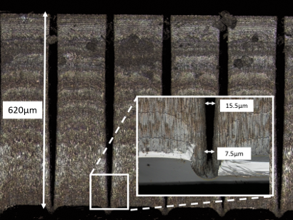
Reference
$^{[1]}$ T. Hasebe et al., “Concept study of optical configurations for high-frequency telescope for LiteBIRD,” J. Low Temp. Phys. 193, 5 (2018).
The Simons Observatory (SO) is a next generation Cosmic Microwave Background (CMB) experiment in the Atacama Desert of Chile that will measure both temperature and polarization at frequencies ranging from 27 - 270 GHz. SO will deploy 60,000 transition edge sensor bolometers across 49 multi-chroic detector arrays. Housed in both large-aperture (6 m) and small-aperture (0.5 m) telescopes, these detector arrays will be coupled to either feedhorn antenna arrays, or hemispherical-lenslet-coupled sinuous antennas. With this dramatic increase in detector count from previous experiments, scalable production methods for the first optical element of the array (lenslet or horn) must be developed. We report on the development of lenslet array fabrication techniques, including the implementation of epoxy-based anti-reflection coating. We will describe the simulations and optical tests of monolithically machined, silicon lenslet array designs with machined, epoxy anti-reflection coatings, and full-array, molded, epoxy anti-reflection coatings for multi-piece array designs.
Transition edge sensors (TES) exhibiting high energy resolution of a single optical photon have been applied to photon-counting microscopy for biological imaging1. We are aiming to develop multi device TES showing large effective area in order to improve measurement efficiency of photon-counting microscopy. We fabricated 3×3 array TES where single device exhibits dimension of 8 µm×8 µm and film thickness of Ti 20 nm and Au 10 nm on Si substrate as shown in Fig. 1 (a). It must be checked whether each device in array TES on Si without membrane structures which keep thermally each device away operates independently or not. At first, we operated the device A and B in Fig. 1 (a) at once to obtain P-V curve of the device A as shown in Fig. 1 (b) PB = 52 pW. Joule power of the device A at 2 devices operating stayed about the same as that at single device operating, PB = 0 pW. Next, we operated the device A and B at once so that power of the device B equaled the sum of power of the 8 devices next to the device A instead of the 9 devices operating at once to obtain P-V curve of device A as shown in Fig. 1 (b) PB = 470 pW. Although joule power of the device A at PB = 470 pW was smaller than that at PB = 0 pW by 21%, electro thermal feedback on the device A at PB = 470 pW worked. Static thermal influence from neighbor devices was revealed. Dynamic thermal crosstalk is investigated by measurement of signal response.
1 K. Niwa et al., Sci. Rep., 7, 45660 (2017).
The observation of neutrino-less double beta decay(0nbb) would be the most practical way to prove the Majorana nature of the neutrino and lepton number violation. CANDLES studies Ca-48 double beta decay using CaF2 scintillator. The detector is currently operating with CaF2 crystals in the Kamioka underground observatory, Japan.
As a next generation detector of the CANDLES experiment, we develop a simultaneous detection method for heat and light signals from CaF2 crystals at mK temperatures. The simultaneous detection using a scintillating bolometer is advantageous for 0vbb search experiments because of its good energy resolutions and strong particle identification capability.
As an R & D of the project, we carried out low temperature experiments with both CaF2(pure) and CaF2(Eu) scintillation crystals using metallic magnetic calorimeter (MMC) technology.
We achieved simultaneous measurement of heat and light signals from a CaF2 crystal for the first time. The signals associated with electron/gamma events were also distinguishable from internal alpha events in the crystal.
We also found ultraviolet scintillation of CaF2(pure) was absorbed in the gold film on the crystal surface resulting in a part of heat signal. The gold film was designed as a phonon collector for the heat channel. This heat signal contribution from light absorption in the phonon-collector film affects the measured energy resolution of about 2% but with some improvement possibility from pulse shape analysis. On the other hand, another set of measurement was made using a CaF2(Eu) which has scintillation in visible region. Improved resolutions and discrimination power were obtained. In the presentation, we discuss the measurement results using both CaF2(pure) and CaF2(Eu) crystals together with future plans for 0vbb applications.
The purpose of COBAND (COsmic BAckground Neutrino Decay) experiment is to determine neutrino mass by measuring neutrino decay photon. Expected neutrino decay photon energy is too small (25 meV) to detect using a semiconductor detector,so we adopted the STJ (Superconducting tunnel Junction) detector using superconductor which has much smaller energy gap than a semiconductor. Our Nb/Al-STJ prototype already satisfied our demands to detect a far-Infrared single photon, but the large noise of readout line inside of refrigerator prevent the detection. For that reason we consider amplifying the STJ's signal by cryogenic amplifier near STJs. We require that the cryogenic amplifier can be operated at lower than 3 K, can amplify fast signal from STJ (<$\rm 10 \mu s$), has low noise (NEP ~$\rm 1×10^{-19} {W/ \sqrt{Hz}}$), and has lower power consumption than the refrigerator cooling capability. Cryogenic amplifier consists of FD-SOI-MOSFET known to operate at cryogenic temperature. The present prototype of a cryogenic amplifier is a charge integrating amplifier with negative feedback. It is composed of an amplification stage and a buffer amplifier. We confirmed that this amplifier worked at cryogenic temperature 350 mK and measured its gain and equivalent input noise charge. I will report the result of amplification with this cryogenic amplifier of Nb/Al-STJ signals by illuminating visible laser pulse.
Axion is a hypothetical elementary particle proposed to solve the strong CP problem in QCD and is one of dark-matter candidates. The sun is considered to emit axions of a continuum spectrum similar to that of blackbody emission with kT~1.3 keV by the Primakoff effect. In addition, line emission is expected through M1 transitions of nuclei; an example is 14.4 keV from $^{57}$Fe (Moriyama 1995). Namba et al., 2007 searched for a 14.4 keV gamma ray from $^{57}$Fe axion absorber with a semiconductor detector and placed on a mass upper limit of QCD axions.
However, the branching ratio from an excited $^{57}$Fe to a 14.4-keV γ-ray is only 9%, and remaining 91% of energy is self-absorbed. The total efficiency is only 1%, if we take the solid angle of the detector into account. Microcalorimeters can detect almost all energy converted from an axion, and thus can improve the detection sensitivity dramatically. Although the mass of the axion absorber of one calorimeter may be much smaller than that of semiconductor experiment, we can increase it by using an array device.
We are thus developing TES microcalorimeters for solar axion exploration. One of the challenge of this research is in ferromagnetism of the Fe axion absorber. We decided to place the absorber at a certain distance from the TES and to connect them with a thermal strap. We have studied the minimum distance required between them with simulations and experimentally measured the R-T curve of an TES with Fe placed at the distance. We then studied the thermal strap design with simulations. The results depend on the thermal conductance of ion at low temperatures. We thus measured the electrical resistivity of Fe films fabricated with electro-deposition to estimate the thermal conductivity. In this paper, we report the optimization of the design of TES microcalorimeter for a solar axion search basing on those simulations and experiments, and the current status of the TES microcalorimeter fabrication.
SuperSpec is a new technology for millimeter and submillimeter spectroscopy. It is an on-chip spectrometer being developed for multi-object, moderate resolution, large bandwidth survey spectroscopy of high-redshift galaxies for the 1 mm atmospheric window. SuperSpec targets the CO ladder in the redshift range of z = 0 to 4, the [CII] 158 um line from z = 5 to 9, and the [NII] 205 um line from z = 4 to 7. All together these lines offer complete redshift coverage from z = 0 to 9. SuperSpec employs a novel architecture in which detectors are coupled to a series of resonant filters along a single microwave feedline instead of using dispersive optics. This construction allows for the creation of a full spectrometer occupying as few as several cms squared of silicon, a reduction in size of several orders of magnitude when compared to standard grating spectrometers. This small profile enables the production of future multi-object spectroscopic instruments required as the millimeter-wave spectroscopy field matures.
The SuperSpec filterbank is coupled to the inductive meander of titanium nitride (TiN) kinetic inductance detectors (KIDs), which serve as the power detectors. The unique coupling scheme employed by SuperSpec allows for the creation of extremely low volume (~2.5 cubic microns), high responsivity, TiN KIDs. Since responsivity is proportional to the inverse of quasiparticle-occupied volume, this allows SuperSpec to reach very low NEPs.
We investigate in detail the noise properties of these extreme detectors. In particular, we examine the scaling of both white noise and 1/f noise with respect to array temperature, loading, volume, and superconducting transition temperature (Tc). We will compare these measurements to analytical models for the expected noise levels. Finally, we will additionally present measured time constants for the SuperSpec detectors.
SPICA is a spatial infrared observatory project proposed by the Japanese spatial agency (JAXA) and selected in May 2018, with two other projects, as M5 medium mission candidate of the ESA Cosmic Vision Program. B-BOP is one the three instruments of this project: a three-band polarimetric imager made of five 16 x 16 pixels matrices and one 8 x 8 pixels matrix.
The B-BOP detector has the particularity of being directly built on its readout circuit, which is used as a mechanical substrate during its manufacturing process. By this mean, the distance between the detector and the readout electronics is minimized, and so the parasitic capacitance of the interconnections. It results that the working temperature of the detector and the readout circuit is the same: 50 mK. This imposes extremely severe constraints on the power consumption of the circuit, with a thermal budget of only 0.1 µW by matrix of 16 x 16 pixels, each pixel requiring 5 readout channels.
The readout circuit that we have designed, ECLIPSE, takes in charge the first “amplification” stage (buffering), and the 16 to 1 multiplexing, of a 16 x 16 pixels matrix. To reduce the power consumption, the input stage of a channel is powered only when it is read, i.e. 1/16th of the time. The impedance of the detector being very high (1 Gohm), a complex sequencing of the clocks has been implemented to avoid charges injection in the detector when switching. The performances of the used technology, CMOS 0.35 µm by AMS, had been previously validated at 100 mK on a technology test circuit. The test of ECLIPSE circuit will start in the coming months, after reception from the foundry.
Film stress has been long known to affect the properties and performances of thin superconductors. In the quantum computing field, a slightly compressive film (~ -100 MPa) has been shown to be ideal for making superconducting-insulating-superconducting (SIS) junctions, no analogous study has been done for superconducting resonators. Anecdotal evidence suggests compressive films show lower loss when patterned as millimeter wavelength transmission lines. We plan to test this relationship using narrow-band microstrip resonators and studying resonator quality factor ($Q$) with film stress, with film stress varying from -700 MPa (compressive) to 300 MPa (tensile). The devices are single-layer Nb lumped-element kinetic inductance detectors (LEKIDs) with resonance frequencies between 0.6-1.7 GHz. Around 200 nm of Nb is deposited onto high resistivity silicon wafer via sputtering under varying chamber pressures and the film stresses are subsequently measured. The wafers are then patterned via optical lithography and dry etched with fluorine plasma. We measure the resonance $Q$ and $T_c$ for each film using a helium dilution refrigerator.
For integrated FET based circuitry in close proximity to the front-end detectors or semiconductor or superconducting qubit generating hardware held at cryogenic temperatures, any transfer of heat produced in the FET circuitry alters the performance conditions of the system and results in noise and spurious signals. Therefore, it is of great interest to analyze and experimentally characterize the processes of heat generation at the transistor level, the heat transport mechanisms from the intrinsic active region of the transistor to the interconnection metal lines, the substrate, and finally the entire circuit itself.
We introduce the analysis and experimental results of the energy consumption, the energy transfer mechanisms, and the process of conversion of electrical energy into heat. The different heat transfer mechanisms that consider the contributions of phonons and electrons, respectively, are modeled as a function of the FET technology parameters including gate oxide thickness, bulk and source/drain doping, and the device geometry and structure. This model serves the purpose of calculating the intrinsic device temperature, the amount of self-heating, and the coupled electro-thermal transport effects at sub-Kelvin temperatures.
We prove that as the temperature is reduced down to the sub-Kelvin regime, more than 70% of the heat in the transistor is transferred by electrons rather than phonons, and that such a heat transfer is a function of the gate oxide thickness, as well as the bulk and source/drain doping levels. The characterization and modeling of the thermal behavior and its coupling to the electrical performance is crucial in determining the electrical-thermal cross coupling. FETs fabricated in 65nm and 14nm CMOS technologies are characterized from room temperature down to 250 mK.
The energy range of transition-edge-sensor (TES) X-ray microcalorimeters with a multiplexed read-out depends upon the width and shape of the TES superconducting transition, and also on the dynamic range of the read-out. In many detector systems, the multiplexed read-out slew rate capability will be the limiting factor for the energy range. In these cases, if we are willing to accept some energy resolution degradation, we can significantly extend the energy range by increasing the bath temperature of operation, essentially creating a second “extended energy range” mode of operation. Increasing the bath temperature reduces the signal size and the peak slew-rate. This makes the pixels easier to readout and can therefore increase the dynamic range to higher photon energies. However, this comes at some trade with intrinsic energy resolution (because of increased thermal noise), increased susceptibility to bath temperature fluctuations and increases the impact of the readout noise. In this paper we explore the trade-off between dynamic range and energy resolution from simply changing the bath temperature of the TES. We present measurements of TES resolution and slew-rate as a function of bath temperature and compare to numerical simulations.
Future cosmic microwave background (CMB) experiments, including the large scale ground based Stage Four CMB Experiment (CMB-S4), satellites, and balloons, aim to map the CMB to an unprecedented precision in order to answer several key questions in cosmology. However, to reach the target noise sensitivity, more than 100,000 detectors will be needed. Microwave Kinetic Inductance Detectors (MKIDs) are ideal detectors for experiments using large number of detectors due to their intrinsic multiplexing capabilities and ease of fabrication. We present fabrication procedure for making a prototype orthomode transducer (OMT)-coupled MKID array optimized for CMB observations. These devices are made from silicon-on-insulator (SOI) wafers. A set of planar OMTs couples the two polarizations of light from our feedhorn to separate Nb/SiN/Nb microstrips, which are then coupled to Al lumped-element KIDs (LEKIDs). The silicon and oxide layer on the backside of the OMT and MKIDs are etched away using deep reactive ion etch (DRIE) for better optical coupling and two-level system (TLS) noise mitigation. We also show the preliminary results from optical and dark testing measurements.
Kinetic inductance detectors (KID) have received increased interest due to their low noise, and scalability to large format arrays required by next generation of astronomical telescopes. The development of KIDs has progressed rapidly, with very low noise equivalent power demonstrated by several groups and KIDs arrays implemented in several ground-based and air-borne instruments. In this paper, we describe a new fabrication process which consists of a membrane isolated KID incorporating a phononic bandgap structure tuned to block recombination phonons from escaping to the thermal bath. This architecture is designed to increase the quasi-particle lifetime and results in increased responsivity to signal photons and lower noise. These devices have been fabricated as lumped-element resonators with hafnium inductors and niobium capacitors on low stress silicon nitride and silicon-on-insulator membranes. We discuss the fabrication process, which uses a combination of sub-micron laser based direct write lithography and nanoscale electron beam lithography.
SAFARI is the prime focal-plane instrument on board the space observatory, SPICA, a candidate for ESA’s fifth medium class mission in its Cosmic Vision science programme, with a planned launch date in 2032. Combining a large, cold mirror with ultra-sensitive detectors (dark NEP $\leq2\times10^{-19}\rm\ W/\sqrt{Hz}$), SPICA/SAFARI will probe the chemistry of the cold, dusty Universe with unprecedented sensitivity, allowing us to trace the evolution of galaxies out to high redshift, as well as the formation of stars and planets in our own Galaxy.
In order to read out SAFARI's ~3600 TES bolometers we use frequency domain multiplexing (FDM). Each TES is in series with a narrow band-pass filter and is voltage-biased by an AC tone tuned to the filter frequency. The resonance frequencies are defined by in-house developed cryogenic lithographic LC filters. Each readout channel comprises a set of ~160 TESs and LC filters and is read out with a SQUID preamplifier. The resulting output is a phase-shifted copy of the applied AC bias tones, amplitude-modulated by each corresponding TES. Baseband feedback is applied to overcome the dynamic range limitations of the SQUID.
We have carried out extensive characterization of the FDM readout system coupled to a 176-pixel TES bolometer array in order to understand the performance, calibration, and crosstalk of the system. Based on these results, we have established the design parameters for the LC filter-chips and TES bolometer arrays fabricated for the next generation of the FDM readout demonstrator. We present our latest results and discuss them in the context of the instrument performance.
A large cylindrical cadmium molybdate crystal with natural isotopic abundance has been successfully used to fabricate a cryogenic microcalorimeter. The measurement was performed above ground at milli-Kelvin temperature, allowing simultaneous readout of the heat and the scintillation light using NTD-Ge sensors. We present its powerful discrimination capability of $\alpha$ versus $\gamma/\beta$ events. The achieved energy resolution has FWHM from 5 keV (at 238 keV) to 13 keV (at 2615 keV). The low internal trace contamination of the $CdMoO_4$ crystal was evaluated as well. The excellent detector performance with preliminary positive indications proves that cadmium molybdate is an extremely promising detector crystal for neutrinoless double beta decay scintillating bolometric experiments with ${}^{116}Cd$ and ${}^{100}Mo$ nuclides in the next-generation technique.
Kinetic inductance detectors (KIDs) are being implemented in more telescopes due chiefly to their excellent sensitivity and natural multiplexability. We have integrated a superconducting nanowire into the resonant circuits, increasing the frequency response, which in turn, increases the sensitivity for single photon detection. Analyzing the frequency response as a function of optical power, we characterize an array of frequency multiplexed superconducting nanowire single photon detectors (SNSPDs). In this paper, we report on the detector's defining properties, including count rate as a function of optical loading, and the response at low optical power, in a thermal quasi particle dominated state. An analysis is given on the quasi particle lifetime, $\tau_{qp}$, using the quasi particle rate equation.
We present simulation software utilizing graphical processing units (GPUs) for the physics of detectors based on arrays of transition-edge sensors (TES).
With the support of GPUs it is possible to perform simulations of large pixel arrays, making the software a powerful tool in detector development.
Comparisons with TES small-signal and noise theory confirm the representativity of the simulated data.
In order to demonstrate the capabilities of this approach we present its implementation in XIFUSIM, a simulator for the X-ray Integral Field Unit, a cryogenic X-ray spectrometer on board the future Athena X-ray observatory.
The GroundBIRD is a telescope aiming a precise observation of the polarization of the cosmic microwave background (CMB) at the Teide observatory in Spain. The E-mode polarization of CMB has been observed by various experiments and provided useful information of the early universe. On the other hand, the B-mode of CMB polarization, which is known to be generated by the primordial gravitational wave from the cosmic inflation of the universe, is not detected yet.
To achieve maximum sensitivity for the B-mode detection, the GroundBIRD telescope adopts two extra features: a fast rotation scanning and application of kinetic inductance detector (KID). The GroundBIRD scans the sky by continuous rotation at a speed of 20 rpm in azimuth direction, tilted by a few tens of degrees from the zenith. This allows us to suppress greatly the 1/f noise. Combining rotation scanning with the rotation of the earth, the total field of view can be larger than 40%, which corresponds to the large angular scales and multipole moment l ~ 6. The focal plane consists of seven modules for two target frequencies, six for 145 GHz band and one for 220 GHz band. Each module has 23 polarization-sensitive antenna coupled KID array. The KID technology allows us to read out order 100 detectors with single ADC. These two advantages enable us to detect or constrain the tensor-to-scalar ratio which parameterizes the energy scale of the inflation, in particular the low l region. In this year the telescope is transported from Japan to Spain, assembled and being commissioned. We present the recent updates, results, and plan of the GroundBIRD experiment.
High resolution spectrographs employed in astronomy and elsewhere use a primary dispersive component to separate light at angles corresponding to different wavelengths, roughly $d\sin(\theta) = m \lambda$. A secondary dispersive component is then used to separate the orders, $m = 0, 1, 2,3...$ By this method, spectral features can be very well separated and detected at high spectral resolution ($\frac{\lambda}{\Delta\lambda} > 5000$) on a planar photo-detector (e.g. a CCD) at the expense instrument volume. In this contribution, we consider the advantages and disadvantages of using a photonic circuit at millikelvin temperatures to achieve the primary dispersive function, and an MKID array to achieve the secondary dispersive and photo-detection functions. At the face of it, this approach could miniaturize spectrograph technology at the expense of low temperature complexity. The native energy and timing resolution of the MKIDs is used to discriminate the orders and provide photon arrival information useful in time-resolved spectroscopy. We describe considerations and formulae involved in the design such a spectrograph.
HOLMES is an experiment with the aim to directly measure the neutrino mass. HOLMES will perform a precise calorimetric measurement of the end point of the Electron Capture (EC) decay spectrum of $^{163}$Ho in order to extract information on neutrino mass with a sensitivity below 2 eV. In its final configuration, HOLMES will deploy 1000 detectors of low temperature microcalorimeters with implanted $^{163}$Ho nuclei.
The baseline sensors for HOLMES are Mo/Cu TESs (Transition Edge Sensors) on SiN$_x$ membrane with gold absorbers. The TES detectors are designed to have an energy resolution of few eV FWHM at the 2.8 keV $^{163}$Ho end-point and to be fast enough to assure a time resolution of 3 $\mu$s, in order contain systematics coming from unresolved pile-ups. Considering the large number of pixels and an event rate of about 300 Hz/pixel, a large multiplexing factor and a large bandwidth are needed.
A promising readout candidate that can fulfill this requirement is the microwave multiplexer, which offers several gigahertz of readout bandwidth per pair of coaxial cables. The TESs are coupled to rf-SQUIDs embedded in superconducting microwave resonators, which are probed via a common microwave feedline and read out at room temperature using GHz signals carried on coaxial cables. This form of multiplexing moves complexity from the cryogenic stages to room temperature hardware and digital signal processing firmware which must synthesize the microwave tones and process the information contained within them. In this contribution we present the basic theory and the considerations of a microwave SQUID multiplexer designed to match HOLMES requirements. Finally the status of the development and the performances currently obtained, in terms of noise, time and energy resolutions, are presented.
The SuperCMDS collaboration uses advanced high voltage Neganov-Luke phonon-assisted detectors for low mass dark matter detection. The leakage current associated with high voltages limits the ultimate sensitivity reach for this large mass detector technology. Although the current leakage performance of the detectors is sufficient for SuperCDMS SNOLAB requirements, improvements are needed to reach the ultimate single electron resolution expected using this technology. We report on recent progress toward understanding the leakage in SuperCDMS-style high voltage detectors and efforts to improve our metal-semiconductor interface design.
B-BOP is one of the three scientific instruments of SPICA which aims, among other scientific goals, to map the galactic filamentary structures and their associated magnetic fields.
Each pixel of B-BOP consists of two orthogonal arrays of dipole antennas supported by four suspended interlaced spirals based on Si :P, B. In order to have a deep understanding of the influence of the doping densities on the Si thermometer’s electrical behavior, we have experimentally investigated, over a wide range of temperatures and with different doping densities, several square Si:P, B samples. The obtained results showed nonlinear R(PJoule) behavior which can be described by the variable-range hopping model. In addition, numerical simulations based on the experimental results, have been carried out to study the thermoelectric behaviour of each pixel as a function of the bias current, Ibias, and the absorbed optical power, POpt. We demonstrated (i) a strong dependence of the detector response, S = dV/dP, with Ibias over a five order of optical power magnitude, (ii) a gain of more than two orders of magnitude in sensitivity over Herschel space observatory, and (iii) a thermal time constant around 70 ms.
We are developing a chemical imaging capability (“Hyperspectral X-ray Imaging”) for microscopic samples based on ultra-high-resolution x-ray emission spectroscopy with large transition-edge sensor microcalorimeter arrays in the scanning electron microscope. By combining microcalorimeter arrays with hundreds of pixels, high-bandwidth microwave frequency-division multiplexing, and fast digital electronics for near real-time data processing, our goal is to enable practical chemical speciation analysis using small-laboratory instrumentation rather than synchrotron beamlines. Our focus is on mapping the detailed chemical form of microscopic particles containing materials from the nuclear fuel cycle. Their detailed chemical form is a crucial link to material origin, history, and behavior in the environment. In combination with developing the instrumentation to obtain high-quality x-ray emission spectra on such samples, we are working to develop a validated theory capability to interpret fine structure in the spectra and better understand fundamental properties of actinide chemical bonding. We will present our approach to developing the Hyperspectral X-ray Imaging capability, recent results from a 128-pixel microcalorimeter array at LANL and the 16-pixel STAR Cryoelectronics MICA-1600 spectrometer, and the path to high-throughput chemical mapping.
The existence of Dark Matter (DM) is supported by astronomical data and observations; however, to date there is no confirmed direct detection of DM. The SuperCDMS collaboration has expanded its capabilities with the development of the prototype HVeV detector. The HVeV detector uses a high voltage applied across the Si (or Ge) crystal to accelerate charges, which scatter off the crystal lattice generating additional phonons via the Neganov-Trofimov-Luke (NTL) effect. The total energy of the generated phonons is equal to the number of e$^-$h$^+$ pairs times the applied voltage, thus the detector response is quantized from the discrete e$^-$h$^+$ pair production. Unfortunately, the accelerated charges can (with some probability) free other loosely bound charges throughout the crystal, referred to as impact ionization. The observed energy from events that undergo impact ionization will not be quantized due to an incomplete NTL effect on the freed charges. These types of events will lie between the quantized peaks and appear as a flat high energy background. Here we discuss a technique for studying the effect of impact ionization on the SuperCDMS HVeV detector using a pulsed laser at ultra-low intensity.
Energy-dispersive low-temperature detectors (LTDs) enable radionuclide spectrometry with energy resolutions exceeding by far those of conventional detectors such as Si(Li) detectors. Also, the energy threshold of radionuclide spectra can be much lower than with conventional techniques. Within the European Metrology Research Project “MetroBeta”, beta spectrometry based on metallic magnetic calorimeters (MMCs) and radionuclide sources embedded in absorbers have been developed. Since this technique requires compatible source/absorber elements that provide optimal detection efficiency and avoid spectrum artefacts, new preparation techniques for reliable source/absorber fabrication have been established and tested.
Laser cutting and milling techniques are used to format noble metal foils with thicknesses ranging from 15 µm to 300 µm into arrays of absorber elements with lateral dimensions of about 0.6 mm to 3 mm. Automated microfluidic dispensing is used to deposit patterns of droplets of the radioactive solution onto the absorber elements. Individual droplet volumes of < 200 pl can be achieved with a high lateral placement accuracy. In this way, a well-defined activity is placed avoiding the formation of large crystals when salt-based carrier solutions are used. Subsequently, the radioactive material must be completely enclosed by the absorber material to ensure the detection of each beta particle and the absorption of the complete decay energy. Diffusion welding of matched absorber elements has been applied to realize such 4$\pi$ source/absorber configurations. Temperature, pressure and processing time were varied to find best conditions that ensure ideal diffusion welding. It was found that this process strongly depends on the source and absorber materials.
The contribution will discuss the details of the source/absorber preparation techniques developed within “MetroBeta” as well as its quality control by means of radiographic imaging and contamination measurements.
Superconducting transition edge sensors (TESs) have demonstrated high detection efficiency and photon-number resolving capability, making TESs attractive in quantum information. The detection efficiency is determined by several factors: fiber-to-detector coupling, absorption of photons in superconducting films, and internal quantum efficiency. The optical absorption of titanium film at the wavelength of 1550 nm, is approximately 30%, determined by its refractive index. Embedding the Ti-based TES in an optical structure to enhance its absorption is an effective approach for improving detection efficiency. We integrated the TES with an optical cavity, consisting of 16-layer dielectric reflection mirror and 4-layer anti-reflection layer, and studied the effect of fabricated optical cavity on the detection efficiency of Ti TES single photon detectors. The critical temperature (Tc) is decreased to 260 mK after deposition of antireflection layer from its original Tc of 350 mK. The detection efficiency (i.e., the ratio of the detected power to input power) was increased up to 30% , thanks to the enhancement of photon absorption by adding the optical cavity.
Refrigerators based on normal metal-insulator-superconductor (NIS) junctions are an attractive solution for cooling superconducting detectors, particularly in balloon- and space-based experiments. The addition of NIS devices to a cryogenic system can enable payload temperatures near 100 mK from launch temperatures near 300 mK. Used in conjunction with a 3He sorption fridge, NIS devices can provide a simple, compact, and reliable cooling chain. Lowering the operating temperature into the 100 mK regime allows for detector designs with lower noise equivalent power (NEP) and higher mechanical robustness compared with many detectors used in past balloon-born experiments. We are presently developing arrays of NIS-cooled transition-edge sensor (TES) bolometers for cosmic microwave background (CMB) science. Each TES in the array relies on cooling from eight NIS junctions, and therefore high junction yield is of critical importance. We present recent work on increasing the fabrication yield of NIS-cooled TES devices by reducing the surface roughness of the SiN-on-Si substrate. Using our in-house grown SiN, we have substantially improved the substrate surface roughness from RMS = 0.75 nm to RMS < 0.4 nm, resulting in fewer shorts in the nm-thick tunnel barriers. Si-rich regions are likely the cause of unwanted roughness peaks in previously-used SiN-on-Si substrates. We demonstrate successful NIS refrigeration of TESs similar to those used on the most-recent camera installed on SPIDER, a balloon-born CMB experiment.
A superconducting transition edge sensor (TES) is used as an ultrasensitive thermometer to measure temperature changes in the range of μK. In the framework of the CRESST experiment (Cryogenic Rare Events Search with Superconducting Thermometers); which is a direct dark matter detection experiment, tungsten TESs are used as the sensing element. Detectors in CRESST are constituted, in brief, of a target crystal with a mass of a few tens of grams. These detectors are operated as cryogenic calorimeters at ~10 mK. The main detection channel is nuclear scattering of hypothetical dark matter particles (or background radiation) inside the target crystal. The deposited energy is then converted into heat leading to a measurable temperature rise in the temperature sensor.
To cope with the foreseen demand for TES, in the current and future phases of the experiment, we investigated the possibility to implement a reliable, simple and reproducible fabrication method using a conventional sputtering system. In the contribution we will present the method under development for tungsten-based TESs using conventional magnetron sputtering with xenon as sputtering gas. TESs with Tc down to 15 mk have been obtained with transition width smaller than 1 mk. We will also give a first assessment on the reproducibility of the process and present the potential for the tuning of Tc.
We target to realise a future satellite mission, LiteBIRD, which will observe full sky at the second Sun-Earth Lagrangian point (L2) and measure the polarisation of the Cosmic Microwave Backgrounds (CMB).
We plan to use Transition Edge Sensor (TES) bolometers to measure the polarisation signal.Measurements of past satellite missions at L2 were disturbed by galactic cosmic rays.Therefore, we need to mitigate the effects from galactic cosmic rays to realise our mission.
Our main concern is the following process:
(1) Cosmic rays deposit energy in silicon substrate where bolometers are.
(2) The energy is propagated by phonons in the silicon substrate.
(3) When some phonons enter a bolometer, the bolometer senses it and spurious signal is created.
In this poster, at first, we show our ideas to mitigate the phonon propagation, as well as the set-up of irradiation test to verify the mitigation ideas.
Next, we show the simulated results of some configurations of parameters using a phonon simulator. Following this, we show the results of irradiation tests,
and compare them to the data from phonon simulations. Finally, we discuss our results and conclude.
Bringing the operating frequency of available single photon detectors down to the microwave regime is an important capability for microwave quantum optics and superconducting quantum information processing. However, this task remains challenging due to the small energy of photons at this frequency compared to room temperature noise. Our circuit quantum electrodynamics (cQED) based detector [1] exploits the superradiant ‘bright’ and subradiant ‘dark’ states that are formed when superconducting transmons are coupled an appropriate distance from each other on a common waveguide [2]. Detuning each transmon inhomogeneously from the operating frequency leads to coupling of the bright and dark subspaces which allows for absorbed photons to be trapped for longer than the inverse of the absorption bandwidth. We utilize this long interaction time to achieve high-fidelity measurements of the photon number in the ensemble leveraging the nearly quantum noise limited amplification of a JPA and Josephson Travelling Wave Parametric Amplifier (JTWPA) in series. Operating the detector at 8 mK and using a single photon source, we benchmark the performance of this protocol. Plans to extend this scheme to GHz bandwidth will also be presented.
[1] B. Royer et al., Phys. Rev. Lett. 120, 203602 (2018)
[2] A. F. van Loo et al., Science 342 1494 (2013)
KIDSPec, the Kinetic Inductance Detector Spectrograph, is a novel concept for a highly sensitive, medium spectral resolution optical through near-IR spectrograph. It uses the intrinsic energy resolving capability of an array of optical/IR-sensitive MKIDs to distinguish multiple orders from a low-resolution grating. By acting as an ‘order resolver’, the MKID array replaces the cross-disperser in an echelle spectrograph. This greatly simplifies the optical layout of the spectrograph and enables longer slits than are possible with cross-dispersed instruments (to improve sky subtraction).
KIDSpec would have similar capabilities to ESO’s highly successful X-shooter instrument. It would provide an R=4000-10,000 spectrum covering the optical and near-IR spectral range (0.4-1.5 micrometers). As well as a ‘long-slit’ mode, the IFU would provide a small (~50 spaxel) field-of-view for spatially resolved sources. In addition, the photon-counting operation of MKIDs and their photon-energy resolving ability enable a read-noise free spectrum with perfect cosmic ray removal. The spectral resolution would be sufficient to remove the bright night-sky lines without the additional pixel noise, making the instrument more sensitive than an equivalent semiconductor-based instrument.
KIDSpec would enhance many existing high-profile science cases, including transient (GRB, SNe, etc.) follow-up, redshift determination of faint objects and transit spectroscopy of exoplanets. In addition it will enable unique science cases, such as dynamical mass estimates of the compact objects in ultra-compact binaries.
CaF2 is a novel target for neutrino-less double-beta decay and spin-dependent dark matter studies, since 48Ca is one of the double-beta decay nuclei and 19F is sensitive to spin-dependent elastic scattering with dark matter.
We implement kinetic inductance detectors(KIDs) on CaF2 crystal which is used as substrate. KIDs on CaF2 is cooled to low temperature with a dilution fridge. The resonance is found in O(1GHz). In addition, several basic parameters of KIDs are measured. Thus, we confirmed that KIDs on CaF2 worked well. This result opens a new possibility in the next generation of astroparticle physics experiments.
We developed a measurement system for simultaneous detection of phonon and scintillation signals from Li2MoO4 crystals based on a metallic magnetic calorimeter (MMC) readout technology. The work was motivated to to check the properness of Li2MoO4 crystals as the main target molybdate crystals for the advance Mo-based rare process experiment (AMoRE). MMCs are one kind of the most sensitive detector technologies used in low temperature detectors. We have studied to surveying a proper scintillating crystal for the final stage experiment that is planning to use 100 kg of 100Mo isotope. Li2MoO4 is one of the promising crystal candidates among molybdate crystals for heat and light detection at mili-Kelvin temperatures. The choice of Li2MoO4 crystal as a target is advantageous in terms of crystal growth and internal background controls. However, its hygroscopic property requires handing care to keep transparent surface conditions. We carried out several sets of measurement using a Li2MoO4 in 5 cm diameter and 5 cm height in dilution refrigerator system. In the presentation we will summarize the difference of the detector performance depending on the surface condition of the crystals. The detector performance including particle identification and energy resolution is to be presented together with feasibility discussion to use Li2MoO4 for 200-kg scale experiment, AMoRE-II.
LiteBIRD is a JAXA-led mission aimed at the studies of B-mode polarization of the cosmic microwave background. Measurements on 15 observing bands from 34 GHz to 448 GHs are made on two instruments, LFT (Low Frequency Telescope) and MHFT (Medium and High Frequency Telescope). To reach the desired sensitivities, more than 4000 TES (transition edge sensors) detectors, used on both instruments, will be cooled to 100 mK. The cryogenic design, based on shield cooling and mechanical coolers is presented in this poster. Shield cooling will be done with passive cooling and mechanical coolers. A single cryogenic chain will cool both instruments. It includes a 4K JT stage cooled with a 4He Joule Thomson cooler from JAXA, precooled by Stirling coolers. Multi-stage ADR will be optimized to provide continuous cooling at 1.75 K, 300 mK and 100 mK. 6 ADR stages provided by NASA and CEA are required and will provide efficient cooling. Details on the thermal design, preliminary sizing and expected performances are presented.
In the current direct dark matter search landscape, the leading experiments in the sub-GeV mass region mostly rely on cryogenic experiments which employ crystalline targets. One attractive type of crystals for these experiments are those containing lithium, such as LiF, Li$_{2}$MoO$_{4}$, and LiAlO$_{2}$. This is due to the fact that $^{6}$Li can absorb neutrons, a challenging background for dark matter experiments, through a distinctive signature which allows the monitoring of neutron flux on site, while $^{7}$Li is the ideal candidate to study spin-dependent dark matter interactions in the sub-GeV region for solid-state experiments.
The measurement of the neutron flux is a significant piece of information for the construction of the background model of an experiment. The adoption of crystals containing lithium would largely improve the current knowledge on the neutron flux in the specific setup. A measurement with a cryogenic detector employing a 373 g LiAlO$_{2}$ crystal has been performed in the first months of 2019 at Laboratori Nazionali del Gran Sasso to assess the feasibility of such a neutron detector.
Additionally, lithium is mostly composed by $^{7}$Li (92.5% natural abundance), an isotope which can be used to probe spin-dependent dark matter interactions alongside the classic spin-independent interactions. First tests designed around this goal were performed in 2018 at Max Planck Institute for Physics in Munich in an above-ground laboratory. The results obtained are extremely promising and support further technological developments headed to explore the dark matter parameter space at low masses.
Th-229 is famous nucleus as the unique candidate of nucleus which can be utilized for realizing nuclear clock. Historically Th-229 is expected to have very low lying isomeric state of less than 10 eV. Existence of 10 eV excited state means the nucleus can be excited by the 124 nm UV LASER. Once the energy level of such isomeric state can be determined precisely by the order of 0.1~0.01 eV, it is realistic to measure the excited state of Th-229 by using LASER Comm technique.
Previously large amount of experimental efforts were made to search for such low lying isomeric state of Th-229 for a long time. Finally, Wense et. al, succeeded to detect the internal conversion electron coming from the Th-229 isomeric state. Later they measured the decay time of Th-229 isomeric state (7 \mu sec).
In this presentation, we present the experimental project to search for the low lying Th-229 isomeric state through the calorimetric measurement of IC electron from Th-229m and/or X-ray from Th-229 29.2 keV state. In order to realize above measurements, we plan to utilize online RI beam so that we can search for the 1st excited state under the clean background condition. The RI beams of Th-229 and Ac-229 are produced with fragmentation separation facility of RIKEN-RIBF. Those beams are degraded, trapped with gas catcher, separated with multi-reflection time-of-flight (MRTOF), and doped in fast TES where X-ray TES is located closely for the measurement of IC decay electron and 29.2keV X-ray from 2nd excited state of Th-229 isomer.
This work is supported by The Japanese MEXT KAKENHI grant No. 18H03713.
We have been developing a microwave superconducting quantum interference device (SQUID) multiplexing (MW-Mux) for the future X-ray astronomical observatory with large field of view and high-resolution imaging spectrometer such as super DIOS (T. Ohashi et al., 2018). MW-Mux consists of a number of superconducting resonators coupled to each dissipationless radio-frequency (RF) SQUID detecting signals from TES X-ray microcalorimeter. Yoon et al., 2018 reported simultaneous readout of 28 pixels, and it is promising that a read out of 100-1000 signals by a pair of coaxial cables.
So far we have been developing MW-Mux with an RF-SQUID coupled directly to a resonator, in contrast to the conventional magnetically coupling regime. The advantage of our directly coupled MW-Mux is a simple chip design based on identical SQUIDs except for the position of grounding via even when all channels are required to have the same gain in the whole readout band, typically 4—8 GHz. Also, we have demonstrated the readout of single-pixel TES X-ray microcalorimeter and the MW-Mux with readout noise lower than 20 pA/$\rm\sqrt{Hz}$ which is below the typical noise level of our TES X-ray microcalorimeter.
In the next stage, we are working on it to increase the multiplexing number. Up to the present, we have designed and fabricated the two chips consisting of 40 resonators in $5\times20$ $\rm{mm^2}$ rectangles, and verified that the 80 resonators and SQUIDs have worked well at 4 K. We have been improving the chip fabrication and microwave circuitry, yielding the enhancement of the unloaded quality factor four times better than before.
Using multi-chip assembly, we are preparing the simultaneous readout of 80 TES X-ray microcalorimeters with our directly coupled microwave SQUID multiplexer.
In this paper, we will report the current status and the latest results of the development of the directly coupled MW-Mux.
We present the progress on the MMC development to be used in the AMoRE project. AMoRE used MMCs as the main readout technology for heat and light detection. The MMCs sensors was first developed based on a gold alloy with 1000 ppm Er. The size of the AuEr sensor material was determined to optimize signal size in the heat channel having a large crystal absorber of about 100 cm^3. Since the measurement is carried out in 10-20 mK, silver based MMC is advantageous in terms of heat capacity in the temperature region. We compared the signal amplitudes of two detector setups with gold foil absorbers in the same size but different sensor materials of an AuEr (1000 ppm) and AgEr (400 ppm). The AgEr sensor resulted in larger signals below 30 mK. Moreover, in the light channel, the size of the AgEr sensor was varied to optimize the light channel with 2inch Ge or Si wafers. We will summarize the test results with tour different sizes of AuEr sensors together with Ge wafer in the same size.
Cryogenic neutrinoless double beta decay searches and low mass particle dark matter searches require a Transition-Edge Sensor (TES) with a high energy resolution. An effective way to improve the energy resolution of a TES detector is to use low-Tc TES. The common practice making a low-Tc TES is using the proximity effect, in which the Tc of a superconducting film is reduced with a normal metal film on one side or with two normal metal films on both sides. The resulting Tc of the bilayer or trilayer TES can be understood by solving the Usadel equations with given boundary conditions. But when solving the Usadel equations in the microscopic description, the electron transparency at the interface or the interface resistance is usually assumed to be a constant (independent on the thicknesses of films). In this paper, we will introduce the film thickness dependence of the electron transparency at the interface, and summarize the modeling results of a bilayer and a trilayer TESs in the microscopic description. Utilizing the experimental data from several resources, including the data from our group and the data in literature, we will compare the fit parameters and fit errors using the model described in this work and the model assuming a constant electron transparency at the interface.
Using microcalorimeters, a high statistics, high resolution calorimetric spectrum of electron capture in ${}^{163}$Ho can be used to determine the neutrino mass. The spectral shape can be calculated from first principles with various assumptions and approximations. To determine the validity of these choices, the theoretical calculations must be compared to data from multiple isotopes. New calorimetric data for a ${}^{193}$Pt-in-Pt absorber measured with a transition edge sensor (TES) are presented and compared to theoretical calculations. In order to create this ${}^{193}$Pt-in-Pt absorber, a ${}^{192}$Pt-enriched Pt foil was irradiated at a nuclear reactor to produce ${}^{193}$Pt in situ. A small piece of this foil was cut off from the bulk foil and attached to an absorber pad thermally coupled to a TES. In this absorber, the radioactive isotope of interest has no elemental interfaces with the absorber material since both absorber and source are Pt, it is uniformly distributed throughout the absorber, and the absorber material is a pure metal. Data from this absorber is useful for understanding the electron capture theoretical shape without the complications of embedding ${}^{163}$Ho in a Au absorber matrix. Calorimetric data from the literature for ${}^{55}$Fe and ${}^{163}$Ho are also compared to theoretical calculations.
Kinetic inductance bolometer represents a sensor technology that can be scaled into large 2D detector arrays. Such detector arrays are attractive for passive sub-millimeter and terahertz imaging systems, providing mechanical simplicity and good-enough imaging capability for terrestrial imaging. We have previously reported on the successful implementation of an imaging system containing a focal plane array equipped with thousands of pixels, optics system and cryogenics operating above 5 K. Here we present a new multiplexing scheme capable of reading the whole detector array with only a modest noise penalty. The readout is called serial addressed frequency excitation (SAFE) as it combines features from both time-domain and frequency-domain multiplexing (FDM) schemes. As a result, the readout is substantially simplified compared to the full FDM case where expensive high-speed digital electronics would be needed. After introducing the readout concept, we describe our implementation of it and show experimental results that verify its performance. Furthermore, video imagery of human subjects at a stand-off of a few meters is presented.
Cadmium-116 is one of the most favourable candidates for neutrinoless double-beta decay (0vBB) searches for two main reasons: first, the energy of the decay (Q = 2813.49 keV) is higher than the end point of the natural gamma radioactivity (2615 keV); then, it can be embedded in CdWO4 crystals, which are efficient scintillators. It was used by the AURORA experiment, which improved the half-life limit on 0vBB decay previously achieved by the Solotvina experiment, by setting a new constraint at 2.2x10^23 years.
In the search that we present here, the 0vBB decay is investigated using a CdWO4 crystal scintillator enriched in Cadmium-116 to 82% as a scintillating bolometer. The detector is installed underground at LSM (Laboratoire Souterrain de Modane) in France. The crystal, which has a mass of 579 g, is coupled to a bolometric light detector in order to collect the scintillation light. The double read-out of heat and scintillation allows us to reduce the background by discriminating between different populations of particles. The main goal of this test is the study of the radio-purity of the crystal and the performance of the detector.
The achieved results are extremely promising. The energy resolution at 2615 keV is 11 keV FWHM at 20.7 mK (to be compared with 163 keV achieved by AURORA with the same crystal operated as a room-temperature pure scintillator). The challenging alpha background can be discriminated with efficiency higher than 99.9%. This result, achieved for the first time with a large-masse enriched crystal, confirms that the bolometric technology provides high energy resolution and background discrimination efficiency, and makes cadmium tungstate one the most promising candidates to investigate 0vBB with this technique.
The SAFARI instrument is a far infrared (34-230 µm) spectrometer on SPICA
(SPace Infrared telescope for Cosmology and Astrophysics), which aims to study subjects such as galaxy evolution and star formation. The transition edge sensors (TES) in the SAFARI instrument are extremely sensitive and are required to have an NEP of $2\times10^{-19}\rm\ W/\sqrt{Hz}$ to ensure background limited observation. It is therefore essential to have a readout system with an output noise that is dominated by the detector noise.
The laboratory amplifier chain currently used to develop the frequency domain multiplexing (FDM) readout system for SAFARI comprises a SQUID (superconducting quantum interference device) and a room-temperature LNA (low noise amplifier). A MHz-frequency calibration tone that causes a known flux excursion in the SQUID is used to measure the total readout noise at different SQUID settings. In order to identify the contributions of the SQUID and the LNA to the total noise we need to know the equivalent current and voltage noise sources of the LNA.
Extracting these noise sources from the measured output noise is rather complicated. This is due to the fact that the output noise depends not only on these noise sources but also on the SQUID noise and the loading impedance at the input of the amplifier, both of which are determined by the SQUID settings. So we need to measure the noise of the LNA separately.
Here we present the output noise of our LNA measured with different resistors ranging from 10 to 400 ohm at different temperatures (50 mK, 1.3 K and 293 K) at the input. The measured data can be well explained with a simple noise model with equivalent noise sources as fitting parameters. We found that that the equivalent current and voltage noise of the LNA are $5.4 \rm\ pA /\sqrt{Hz}$ and $350 \rm\ pV /\sqrt{Hz}$ respectively, both of which are low enough to read out a sensitive TES array.
We present a noise model of the cryogenic High Electron Mobility Transistor developed at C2N laboratory. The model is based on dedicated measurement of voltage and current noises at temperature in the 1K-10K range. The model shows that 10 eV rms and 20 eVee rms could be obtained on the heat channel and ionization channel of massive semiconductor detector operated at low temperature.
Such performance is of high interest for both Coherent Electron Elastic Neutrino Nucleus Scattering (CENNS) experiment such as Ricochet and Dark Matter direct detection experiment such as EDELWEISS. It would allow to probe sub-keV nuclear recoils as induced by sub-GeV/c2 WIMPs and MeV neutrinos from nuclear reactor while retaining electromagnetic background discrimination.
The axion is an excellent dark matter candidate motivated by the Peccei-Quinn solution to the strong-CP problem.The research group of the Center for Axion and Precision Physics Research (CAPP) of the Institute for Basic Science (IBS) in Korea is searching for axion dark matter through several haloscopes experiments. The method, suggested by Prof. P. Sikivie, exploits the axion conversion in microwave photons, via the inverse Primakoff process, using a high-quality microwave cavity permeated by a strong magnetic field. By properly tuning the resonant frequency of the cavity over a certain interval it is possible to cover axion masses in the range of interest. One critical parameter for detecting the feeble signal due to the interaction of an axion is the noise level, which is also responsible for the main source of background in such experiment. To maintain the thermal noise as low as possible, the entire system works at cryogenic temperatures, from 4 K to 50 mK.The latest results obtained in the optimization and characterization phase of these parameters to enhance the experimental sensitivity will be discussed in this contribution.
We report on the observation of frequency up-conversion gain in superconductor-insulator-superconductor (SIS) tunnel junctions at millimeter wavelengths. So far, SIS tunnel junctions have been used as frequency down-converters with the ultra-low noise performance approaching the quantum limit and have exhibited positive gain in the down-conversion process. In principle, it is also possible to operate SIS tunnel junctions as frequency up-converters with ultra-low noise and positive gain. Our proposal is to use SIS junctions as a frequency up-converter in a novel microwave amplifier in combination with an SIS down-converter. Given that both SIS mixers (up- and down-converters) pumped by an local oscillator signal have positive conversion gains and were connected in cascade, input and output frequencies are identical with a signal gain, which has been demonstrated by our proof-of-concept test module [AIP Advances, vol. 8, no. 2, Art. no. 025206 (2018)]. For detailed analysis to improve the performance, it is important to investigate characteristics of the SIS up-converter itself. So, we have developed a test setup to measure frequency up-conversion gain in SIS tunnel junctions at millimeter wavelengths. A conventional SIS mixer with Nb/AlOx/Nb tunnel junctions was used as a frequency up-converter, which has a 20-dB input attenuator and a stainless steel WR-10 output waveguide in a 4-K cryostat. An up-converted signal from the cryostat is measured by a room temperature down-converter system with the double sideband (DSB) noise temperature of about 800 K calibrated for hot and cold loads. We observed distinct intermediate frequency responses to signal inputs from a microwave noise source (with a typical excess noise ratio of 21 dB) biased on and off, which indicated that DSB up-conversion gain in SIS junctions to be positive. Results with a continuous wave source will also be reported.
Sub-mm wave on-chip filter-bank spectrometers disperse THz radiation by means of shunted band-pass filters whose ideal frequency response is a matched-filter to the Lorentzian-shaped spectrum of broadened extra-galactic emission lines, resulting in a resolution requirement of $R=f/\delta{f}\sim{}500$. Furthermore, the instantaneous bandwidth of operation should be as wide as possible to allow for blind spectroscopic scans. For the implementation of these filter-banks we studied in detail co-planar filters, consisting of a single patterned superconducting film, and microstrip filters. A filter with $R=500$ needs to have a low enough loss ($1/\tan\delta = Q_i>5000$) to limit unwanted signal attenuation. We found that co-planar filters are strongly limited by radiation losses, especially for sub-mm waves. Hence, we designed in Sonnet a filter based on a microstrip half-wave resonator, free from spurious resonances within an octave band. For the dielectric we use PECVD a-Si, with a measured $Q_i∼10^4$. The high stress of a-Si sets however a maximum thickness of ~300 nm, which imposes sub-micron featured filters. With the aid of a circuit model developed in-house we predict the interaction between filters when arrayed in a filter-bank configuration. This code made obvious three extra requirements for large filter-banks: (1) a low reflection off-resonance per filter is needed (reflection <-20 dB), (2) the high frequency filters must lead in the filter-bank to limit their losses, and (3) the inter-filter spacing in the thru-line must be $\lambda/4$, and cannot be a higher odd multiple, in order to avoid the coherent addition of reflections from the filters to fall within an octave band. Based on these constraints we designed a filter-bank with 347 efficient channels sampling an octave bandwidth (220-440 GHz) with a resolution of $R=400$. A set of demonstrators with narrower bandwidth are being fabricated and their measurements will follow.
SPT-3G is a third-generation camera for the South Pole Telescope that uses a trichroic pixel architecture and ~16,000 transition-edge sensor (TES) bolometers to map the polarization of the cosmic microwave background (CMB). After successfully observing since January 2017 using TiAu TES bolometers, in December 2018, we replaced one of the ten 150mm detector wafers that comprise the focal plane with a wafer using AlMn-alloy TESs. The AlMn design is likely to be used in future CMB experiments such as CMB-S4. We summarize the fabrication of these sensors and describe their performance both in lab tests and on-sky as part of SPT-3G. The critical temperature, resistance, saturation power, noise, and optical efficiency of the new AlMn wafer are comparable to the existing TiAu devices and meet the requirements of the SPT-3G camera.s and meet the requirements of the SPT-3G camera.
We present an investigation of frequency up- and down-conversion processes in a superconductor–insulator–superconductor (SIS) tunnel junction. A quasiparticle SIS tunnel junction potentially allows positive conversion gain in the down-conversion process from a millimeter wave to a microwave. Recently, we experimentally found that the tunnel junction can also up-convert a microwave signal to a millimeter-wave signal with positive conversion gain. Based on the bilateral gain in the SIS up- and down-conversion processes, we proposed a novel microwave low-noise amplifier and demonstrated the proof of concept. The amplifier uses SIS up- and down-converters which were connected in cascade and driven by a local oscillator (LO) power.
In order to design the amplifier with low noise and high gain, it is important to accurately evaluate and characterize both the SIS converters at radio frequency (RF) and intermediate frequency (IF). However, in general, the evaluation of cryogenic devices at millimeter-wave and even microwave frequencies has been carried out based on a module approach. In this case, the measured conversion gain and impedance are affected by interconnections and interfaces of the package, e.g. connectors, bonding wires and transmission line. This requires correction of the measured values to extract device parameters, which makes uncertainties.
We have evaluated SIS tunnel junctions to estimate specific capacitance using a 4-K cryogenic probe station, which allows us to directly measure S-parameters. In this study, we extend the on-wafer measurement system to directly evaluate SIS up- and down-converters by injecting an LO power at around 40 GHz and adding low and high pass filters to separate the RF and IF signals.
In the conference, the characterization method and the properties of the SIS converters will be presented.
A large array of Transition-edge Sensors (TES) is currently in development as an X-ray spectrometer for the Linac Coherent Light Source II (LCLS-II) at SLAC National Laboratory. LCLS-II is a fast (100 KHz) pulsed X-ray laser that will be almost 1000x brighter than its predecessor, LCLS-I. The combination of high-throughput TES X-ray detectors with this high-luminosity light source will enable us to study the dynamics of chemical reactions with unprecedented resolution. As part of the development process, it has been critical to understand the optimal way to operate a TES detector under extremely high photon fluxes with short pulse times. We will describe the fundamental challenges of pairing a slow microcalorimeter such as the TES with a bright ultrafast X-ray source, and creative solutions to maximize the science reach of LCLS-II. Detailed science projections will be presented along with a comparison to existing X-ray detectors.
On-chip spectrometers, such as DESHIMA and SuperSpec, require transmission lines with $Q_i>10^4$ to achieve sufficient system efficiency. Transmission lines with lower $Q_i$ would introduce too much losses in the line from antenna to filter and in the filters themselves. Data regarding the losses of transmission lines at THz frequencies and sub-K temperatures is severely lacking. An on-chip Fabry-Pérot resonator can be used to measure the internal losses, $Q_i$, of a transmission line with high sensitivity at high frequencies. To create the in-line Fabry-Pérot resonator, a transmission line of certain length is coupled to an THz source via a twin-slot lens antenna on one side and to an Al-NbTiN hybrid MKID on the other side.
We show the detailed design of the Fabry-Pérot resonator to measure the losses of a dielectric in the order of $10^3 < Q_i < 10^5$. There are several experimental challenges for measuring $Q_i$. The first challenge is the limited frequency resolution of the source, due to which resolving high $Q$ can become impossible. Secondly we experimentally found that there is stray light coupled to the detector which causes a spurious response with a level of $-30dB$ with respect to the peak transmission of the Fabry-Pérot resonator. Taking these experimental challenges into account we design an on-chip Fabry-Pérot resonator for measurements of high $Q_i$ dielectrics. In this design we optimize the length, the mode number and the couplers of the resonator. Furthermore we use multiple resonators on a single chip, each coupled to a separate antenna and detector, with different $Q_c$ values. This design method is applicable for different dielectric materials and different transmission line configurations. Using this method we designed and fabricated a chip with which we measured a $Q_i\approx 10^4$ @ 350 GHz for a PECVD deposited a-Si dielectric.
Low-temperature Nuclear Magnetic Resonance (NMR) samples offer long-lived quantum states that are extremely sensitive to small perturbations from new physics, including interactions with axion dark matter. The sensitivity of NMR axion detectors is sometimes limited by the precision with which the magnetization of the spin state can be read out, especially when large geometric pickup coil inductances cannot be tuned because of geometric constraints. DC SQUIDs have been used for high-sensitivity readout of NMR samples, but their "energy sensitivity" is limited to a few quanta, such that $ S_{\Phi \Phi}/2L = n\hbar $, where $n > \sim 1$. Flux sensors with better energy sensitivity (potentially better than $\hbar$) require a different readout paradigm. This work describes the Radio Frequency Quantum Upconverter (RQU), a quantum sensor which uses a dispersive readout scheme to allow better energy sensitivity. In the RQU, the low frequency (kHz-MHz) spin magnetization signal modulates the phase of a microwave readout tone. This scheme allows better energy sensitivity than is possible with DC SQUIDs for applications with untuned reactance, improving the sensitivity of NMR axion detectors.
Total decay energy spectrometry (Q spectrometry) with cryogenic detectors is a promising technique for analysis α-emitting actinides. The radioactive sample is embedded in a 4 pi absorber, and the total decay energy (Q value) for each disintegration is measured. The energy spectrum is therefore simple: there is one peak per radionuclide corresponding to the Q value. The high energy resolution of cryogenic detectors is sufficient to distinguish the peaks at the different Q values. However, this technique is very sensitive to the self-absorption of the nuclear recoils in the source material, it can degrade the energy resolution and can produce peaks with unpredictable shapes.
Like in alpha spectrometry, electrodeposition of the source would be preferable to minimize the self-absorption. Nevertheless, it adds more complexity to the technique and the electrodeposition yields change the proportion of the different elements. Drop and dried deposition of solution is simpler, but it makes sources with inhomogeneous salt crystals with micrometric dimensions. In order to keep the simplicity of drop deposition and to overcome the problem of the source quality, we develop nanoporous gold (NPAu) in which the source solution is dried in a nanometric scale.
A MMC prototype was built with an absorber containing the NPAu and a mixture of Pu isotopes. The synthesis of the NPAu with pores sizes of few tens of nm will be presented with SEM images. In addition, the tests of wetting with radioactive solutions will be shown. From the Q spectrum, the composition of Pu isotopes and other actinides was measured; it is in very good agreement with the reference values given by alpha and mass spectrometry. The Q peak shapes are identical and described by the convolution of a Gaussian and a sum of two left-sided exponentials. However, the FWHM resolution of 7.2 keV is far from the expected resolution of the detector (~1 keV). We will discuss how to improve it in the future sample preparation.
Frequency-Division Multiplexing (FDM) is the baseline readout system for the large array of superconducting Transition-Edge Sensors (TES's) under development for the ESA X-IFU instrument on the future Athena X-ray telescope.
Excellent single pixel performance has been demonstrated already with MHz biased MoAu NASA-Goddard TESs and energy resolution below 2eV @ 6keV is routinely observed, in single pixel mode, with the FDM read-out developed at SRON/VTT.
Non-uniformity in the superconducting transition, due to the Josephson effects in a MHz-driven TES, has been observed and is potentially affecting the performance of a large array readout with a large multiplexing factor.
We are currently testing, under ac bias, several detector arrays fabricated at NASA-Goddard using MoAu-based TESs and at SRON using TiAu bilayers.
In this paper, we will present the results of an extensive experimental characterization of many pixels with various design and electro-thermal properties.
We report on the status of our development of dark matter detectors in which the recoil energy deposited in a crystalline substrate is sensed via the absorption of athermal phonons in kinetic inductance detector (KIDs) (cf. Moore et al 2012, Cornell et al 2014, Chang et al 2018). KIDs are highly multiplexable, offering the prospect of tens or even hundreds of phonon sensors per kg-scale substrate. Such finely pixelated imaging of the phonon signal has the potential for extremely high-fidelity position reconstruction, in particular reconstruction of both radial and z position as well as reduced misreconstruction of surface events as events in the bulk substrate fiducial volume. Our design currently consists of 80 Al KIDs coupled to a Nb coplanar waveguide feedline on a 75-mm diameter, 1-mm thick silicon substrate, a design straightforwardly scalable to thicker substrates (1 cm and larger) and thus to 0.1-1 kg substrate mass. To date, we have demonstrated high fabrication yield, well-controlled resonator frequency placement, and good agreement of resonator behavior with Mattis-Bardeen theory. We are using a novel readout pulsing technique to generate energy deposition in a controlled, localized fashion (see Y.-Y. Chang et al, this conference) in order to measure energy resolution and quasiparticle lifetime. We are engaged in efforts to reduce incident blackbody radiation in order to obtain maximal quasiparticle lifetimes, of order 1 ms and longer, with the expectation of demonstrating an energy resolution below 100 eV. Near-term future work will include integration with a quantum-noise-limited kinetic inductance parametric amplifier and development of an alternate design optimized for energy resolution rather than position reconstruction.
High-resolution X-ray microcalorimeters are challenging to characterize and calibrate at low energies because of the difficulty of obtaining narrow calibration lines approaching the detector resolution. Short pulses of optical light, e.g. generated by a 405 nm laser diode, can be used to provide combs of very narrow calibration lines for TES detectors as long as the detector can resolve the photon number. We have recently demonstrated this scheme for high resolution X-ray micro-calorimeter pixels for photon numbers up to about n=130, i.e. about 400 eV. However, we found that the valleys between integer photon numbers fill in with increasing photon number so that for energies above 0.4 keV the photon number could not be resolved.
Here we describe ongoing work to identify the mechanism causing the degradation and discuss the prospects of extending the technique to higher energies.
SuperSpec is an ultra-sensitive on-chip spectrometer for mm and sub-mm wave observations of high-redshift dusty galaxies. The device employs a filterbank architecture in which kinetic inductance detectors (KIDs) are coupled to mm-wave resonant filters along a single microwave feedline. We present the progress on several advances to the SuperSpec filter bank technology that will be crucial for future far-IR missions. In particular, we present the characterization of a prototype filterbank utilizing thin film aluminum (Al) KIDs for higher sensitivity compared to previous titanium nitride (TiN) devices. In addition, in order to target higher resolving power ($R \sim 3000$), we must reduce filterbank dielectric losses ($Q_{loss} \sim 2 \times 10^{4}$). We will pursue two technologies using a silicon (Si) inner layer dielectric over the current silicon nitride (SiN). First, amorphous silicon (a-Si) offers simple fabrication and low loss at low power. Second, crystalline silicon (c-Si) presents a more challenging fabrication process, including a “flipped-SOI" process using silicon-on-oxide wafers, but has been shown to have $\tan \delta $ as low as $5 \times 10^{-6}$. Finally, in order to push the SuperSpec filterbank technology frequencies up to 1.3 THz, we require a higher $T_{c}$ film replacement for our niobium (Nb) microstrip. For this purpose, we offer preliminary data on niobium titanium nitride (NbTiN) and niobium nitride (NbN) films.
The Large Scale Polarization Explorer (LSPE) is a cosmology program for the measurement of large scale curl-like features (B-modes) in the polarization of the Cosmic Microwave Background. Its goal is to constrain the background of inflationary gravity waves traveling through the universe a t the time of matter-radiation decoupling.
The two instruments of LSPE are meant to operate synergically by covering a large portion of the northern microwave sky. LSPE/STRIP is a coherent array of receivers planned to be operated from the Teide Observatory in Tenerife, for the control and characterization of the low-frequency polarized signals of galactic origin; LSPE/SWIPE is a balloon-borne Stokes polarimeter based on 330 large throughput multi-moded detectors, designed to measure the CMB polarization at
150GHz and to monitor the polarized emission by galactic dust above 200GHz.
Both instruments are in due course of development. We here report the status of the STRIP pre-commissioning phase and the progress in the characterization of the key subsystems of the SWIPE payload (namely the cryogenic polarization modulation unit and the multi-mode TES pixels) prior to receiver integration.
The measured perfomance and the expected level of systematics mitigation allow to constrain B-mode presence down to a tensor/scalar ratio of 10^-2.
Metallic magnetic calorimeter (MMC) technology is a leading contender for detectors for the Lynx X-ray Microcalorimeter, which is an imaging spectrometer consisting of an array of greater than 100,000 pixels. The fabrication of such large arrays presents a challenge when attempting to route the superconducting wiring from the pixels to the multiplexed readout. If the wiring is designed to be planar, then an aggressive, submicron scale wiring pitch has to be employed, which is technically challenging to design and fabricate on account of the requirements of low inductance, low cross-talk, high critical currents and high yield. An alternative way to achieve large scale, high density wiring is through the use of multiple buried metal layers, planarized by Chemical Mechanical Planarization. This approach is well-suited for connecting thousands of pixels on a large focal plane to readout chips, and also for fabricating sensor meander coils with narrow line widths, which helps in increasing the sensor inductance and thus alleviates stray inductance issues associated with the wiring in large size arrays. In this work we describe the fabrication of high sensor inductance MMC arrays implementing Lynx concepts and incorporating multiple layers of buried Nb wiring. The detector array is composed of three sub-arrays with pixels optimized to meet the different science driven performance requirements of Lynx. In two of the sub-arrays we adopt a thermal multiplexing scheme to read out pixels by coupling 25 absorbers to a single sensor through thermal links of varied thermal conductance. We demonstrate the successful fabrication of multi-absorber MMCs with fine pitch pixels in very large size arrays.
The X-ray Integral Field Unit (X-IFU) will operate an array of more than 3000 Transition-Edge Sensor pixels at 90 mK with an unprecedented energy resolution of 2.5 eV at 7 keV. In space, primary cosmic rays and secondary particles produced in the instrument structure will continuously deposit energy in the detector wafer and induce fluctuations of the pixels' thermal bath. In this contribution, we investigate by simulation of the X-IFU readout chain how these fluctuations eventually influence the energy measurement of the science photons.
Realistic timelines of thermal bath fluctuations at different positions in the array are generated from the result of a thermal model and the expected distribution of the deposited energy of the charged particles. We then model the TES response to these thermal perturbations and compute their influence on the on-board energy reconstruction process. Overall, we show that with a proper heatsinking design, the main energy resolution degradation effect remains minimal and within the associated resolution allocation of 0.2 eV. We further study how a dedicated triggering algorithm could be put in place to flag out the rarer large thermal events.
We are developing high resolution transition edge sensor (TES) microcalorimeters for the Athena X-ray Integral Field Unit (X-IFU) instrument. The x-ray absorbers of the TES pixels must provide high quantum efficiency (QE) for the incident x-rays and high reflectivity to longer wavelength radiation. Our pixel designs use ~ 5 micron thick electroplated Au-Bi absorbers. The thickness of the Au and Bi layers are tuned to provide the desired pixel heat capacity and the vertical QE. The high heat capacity Au layer provides fast thermal diffusion of the x-ray energy to the TES and the Bi layer provides additional QE without adding significant heat capacity. In this paper we present the optimization of the absorbers for applications such as X-IFU. To calculate the QE precisely, we have included the effects of surface roughness, edge profile and filling factor of the absorbers and the effects of the different angles of incidence of the incoming x-rays from the X-IFU optic. The surface roughness of the top Bi layer, measured by using an optical surface profiler, was found to have negligible effect on the average QE. To improve the reflectivity of absorbers to low energy radiation we have introduced an Au capping layer on top of the Bi layer. This makes TES detectors less sensitive to shot noise from low energy photons, reduces stray power and eases the design of optical blocking filters. Reflectivity measurements in the wavelength range 300 nm - 20 microns show a significant increase in reflectivity compared to bare Bi layer. This is consistent with the expected reflectivity difference of bulk Au compared with bulk Bi. Characterization of TES pixels with and without the Au capping layer showed no evidence that the capping layer affects the absorber thermalization properties.
Cryogenic lumped-element resonators are near-optimal detectors of the electromagnetic interactions of ultralight (sub-μeV), wavelike dark matter candidates, including axions and hidden photons. Operated as classical detectors, they have sensitivity to well motivated regions of dark matter parameter space, including the QCD axion band at masses from 10neV to 1 μeV. Quantum coherent measurement techniques can dramatically improve their sensitivity and allow them to probe the QCD axions at lower masses, motivating the development of quantum sensors that operate in the appropriate frequency range (below ~300MHz). The Radio Frequency Quantum Upconverter (RQU) is a quantum sensor capable of implementing a variety of quantum coherent measurement techniques in this frequency range, including two-mode squeezing, sideband cooling, and backaction evasion. I will describe the implementation of an RQU with Josephson junctions and superconducting microwave circuit elements and quantum coherent measurement protocols appropriate for reading out a resonant dark matter detector with an RQU.
Discovery of neutrino oscillations revealed that neutrinos have mass, but the absolute mass of the neutrinos still remains unknown. Since neutrinos are a massive particle, a heavier neutrino may decay into a lighter one with a photon emission. The photon energy is expected to be around 25 meV at maximum. The COsmic BAckground Neutrino Decay (COBAND) experiment aims at detecting the photons as decay products of cosmic neutrino background (C\nuB) and determining the neutrino mass. In addition, if we observe excess photons in the C\nuB decay from the prediction by the standard model (SM), it will indicate a physics beyond the SM. Therefore, the detector required in the COBAND experiment is to be capable to measure single photons with a resolution better than 2% at the energy of 25 meV to identify the photons from the two-body decay of neutrinos. Since semiconductor-based detectors cannot satisfy this requirement, we consider using superconducting tunnel junction devices based on hafnium (Hf-STJ), which is known to have the smallest superconducting gap at typical temperatures of low-temperature detector instrumentation. We have established dependable fabrication method to form a SIS structure of Hf-STJ. We also observed pulsed visible photons using the Hf-STJ devices. The leakage current, however, was still found to be much larger than 10 pA of the COBAND requirement. Here we report on the latest measurement and the recent progress of Hf-STJ development for small junction devices. We will discuss the junction-size dependence of the leakage current together with fabrication details on the sputtering conditions of Hf and oxidization method to form an insulation layer. Moreover, we will present the 6 keV x-ray responses measured in an adiabatic demagnetization refrigerator.
We explore the use of cryogenic detectors as the energy resolving component of a laboratory transmission EXAFS instrument. EXAFS (Extended X-ray Absorption Fine Structure) is a powerful X-ray technique that gives element specific information about the structure of molecules. It has the enormous advantage that it does not need a specialized sample form, such as a crystal, and so it can be generally applied to a wide range of fields such as catalysis, materials science, biochemistry, etc. It is currently only available at synchrotron radiation lightsources, where science tends to be restricted to high-profile experiments and by the limitations of working at a remote facility. The development of a laboratory EXAFS spectrometer capable of measuring transmission spectra would be a significant advance which should enable new science and novel applications. Such a laboratory EXAFS instrument could combine a high-resolution, energy-resolving, cryogenic X-ray detector with a broadband X ray generator to measure a transmission spectrum of a sample placed between the generator and detector. In this work, we examine the energy resolution, count-rate, and detector stability needed for good EXAFS spectra in such an instrument. We compare these to those of existing cryogenic technologies and show that the properties of Superconducting Tunnel Junction (STJ) detectors are well-suited for this application. A multi-pixel STJ array capable of operating in the typical EXAFS energy range of 3 – 12 keV would be a novel device, and we propose development paths based on STAR Cryoelectronics’ existing commercial STJ platform.
We are developing a detector array for astronomical observation in
100-GHz band using Microwave Kinetic Inductance Detector (MKID)
and a readout system for the array with frequency sweeping scheme,
which uses a frequency sweeping probe signal instead of a
fixed-frequency probe signal. This scheme enables us to obtain
resonance spectra of MKIDs in an array simultaneously and to derive
the resonance frequencies related to the power of incoming radiation.
It has the advantage that the derived resonance frequencies are not
affected by changes of gain and delay in the transmission line. The
resonance profile measured, however, can be distorted by frequency
sweeping, and it is necessary to evaluate the effect of frequency
sweeping on resonance spectrum. We made measurements using the scheme
with several frequency-sweep velocities and checked dependence of the
resonance frequency and the Q-factor on it. A slow frequency sweep
causes only small difference of resonance spectrum from an ideal
profile, and is suitable for astronomical application.
The application of transition edge sensors (TESs) to exotic atom X-ray
spectroscopy requires challenging techniques of measurement and
analysis. We have developed them through the pionic and kaonic atom
X-ray measurements with a 240-pixel TES array at hadron beamlines.
One of the important analyses is to investigate the charged particle
impacts on the TES array. The energy deposits of charged particles on
the array, especially on its silicon substrate, can cause small
thermal cross-talk pulses in all TESs. The pileup of the thermal
cross-talk and normal X-ray pulses degrades the energy resolution due
to poor pulse-height estimation via optimal filtering.
Recently we have found the shorter record-length analysis for the
piled-up pulses can improve the energy resolution (e.g., more than 1
eV at 6.9 keV). Generally, the optimal filtering for longer
record-length pulses without pileup contamination results in better
energy resolution. However, for the piled-up pulses, the benefit from
cutting the pileup region is bigger than the degradation due to
shorter records.
Here we will show the analysis details and the detector performance of
the kaonic helium X-ray measurement at J-PARC (Ibaraki, Japan). We
will discuss the influence of charged particle impacts on the TES
array to the optimal filter, the pulse-height estimation, the
background events, and the energy calibration. These analysis
techniques and the characterization of TES response to charged
particle impacts must be useful for future experiments at accelerator
beamlines and space missions.
MUSCAT (the Mexico UK Submillimetre Camera for AsTronomy) is a 1.1-mm receiver currently in the final stages of development and scheduled for deployment on the Large Millimeter Telescope (LMT) on Volcán Sierra Negra in Mexico during the third quarter of 2019. In its first generation, MUSCAT will use 1,500 LEKID detectors to carry out follow-up observations of Herschel-ATLAS fields. However, beyond this MUSCAT is designed to offer a versatile platform capable of acting as an on-sky demonstrator for emerging and next-generation detector technologies. To realise this ambition, MUSCAT utilises a combination of continuous sorption coolers and a miniature dilution refrigerator to cool its detector stage to approximately 100 mK continuously. This cryogenic system gives MUSCAT the capability of operating narrow-spectral-band detectors such as multichroic pixels or on-chip spectrometers with background-limited performance. Here we present results for the cryogenic performance of MUSCAT from the final stages of lab commissioning prior to deployment. We will also present the current status of the MUSCAT instrument as a whole and our schedule through to deployment on the LMT.
Superconducting sensors for millimeter and submillimeter astronomy require thin dielectric films. The dielectrics SiO2 and SiNx are currently used for these applications for fabrication convenience reasons. However, they have a loss tangent (tan δ) close to 1e-3. The loss tangent is a critical parameter for these applications because it determines the microstripline's attenuation and the spectral resolution of superconducting spectrometers. The TLS noise of such high-loss dielectrics is too high for them to be incorporated into parallel-plate capacitors (PPCs) for KIDs. Lower loss dielectrics are thus highly desirable, with a loss tangent of 1e-4 or less. To achieve this goal, two low-loss dielectrics are being investigated, crystalline silicon (cSi) and hydrogenated amorphous silicon (a-Si:H). We are undertaking a systematic survey of loss tangent and TLS noise for a-Si:H, virgin c-Si, and wafer-bonded c-Si at both ~1-2 GHz and 100-400 GHz, and here we report on the RF measurements. We fabricated niobium LC resonators with PPCs, incorporating the various dielectrics in the PPC structure. By analyzing the resonance frequency of these resonators at different temperatures (between 250 mK and 400 mK), and for different readout powers, it is possible to deduce the low-power loss tangent, the loss tangent at high readout powers, and the TLS noise of these dielectrics. We present measurements of loss tangent and TLS noise for films with different thicknesses, compare a-Si:H and c-Si, and measure the impact of wafer-bonding. Future work will correlate these results with 100-400 GHz measurements. This study contributes to the development of new low-loss dielectrics in future superconducting sensors for millimeter and submillimeter astronomy, and is expected to provide significant improvements in terms of sensitivity and design architecture possibilities.
Due to their excellent energy resolution, the intrinsically fast signal rise time, the huge energy dynamic range and the almost ideally linear detector response, metallic magnetic calorimeters are very well suited for a variety of applications. In particular, the ECHo experiment aims to utilize large-scale MMC based detector arrays to investigate the mass of the electron neutrino. However, reading out such arrays is a challenging task which can be tackled using microwave SQUID multiplexing. Here, the detector signals are transduced into frequency shifts of superconducting microwave resonators which can be deduced using a high-end software-defined radio (SDR) system.
The ECHo SDR is a custom-made modular electronics. It provides 400 channels equally distributed in a 4 to 8 GHz frequency band where each channel has 1MHz bandwidth. The system consists of a two-stage RF mixing, a modular conversion, and an FPGA board. The mixing board combines/splits five 800 MHz base-bands to/from one single 4 GHz RF-band. For conversion, five two-channel 1 GSPS AD9680 ADCs and three four-channel AD9144 DACs are utilized. The digital signal processing is computed on the custom HiFlex-2 FPGA board. For channelization, a novel heterogeneous approach utilizing the integrated digital down conversion (DDC) of the ADC, a polyphase channelizer followed by another DDC for demodulation is proposed. This offers an efficient channelization resource wise while offering excellent channelization properties. After signal demodulation, on-FPGA flux-ramp demodulation processes the signals before streaming it to the ECHo-100k backend. Calibration and slow-control are handled by the Zynq’s ARM processors, directly on the platform.
Within this contribution, we discuss the current development status of the individual system components of the ECHo SDR. This also includes demonstration experiments for which prototype setups has been built, e.g., for evaluating the novel channelization approach.
Micro-Spec (μ-Spec) is a direct-detection spectrometer that integrates all the components of a diffraction-grating spectrometer onto a ∼10-cm$^2$ chip using superconducting microstrip transmission lines on a single-crystal silicon substrate. The second-generation μ-Spec has been designed to operate with a spectral resolution of ∼512 in the far-infrared and submillimeter (420–540 GHz, 714–555 μm) wavelength range, a band of interest for NASA’s EXperiment for Cryogenic Large-Aperture Intensity Mapping (EXCLAIM). EXCLAIM will be a high-altitude balloon mission that is being designed to map the emission of redshifted carbon monoxide and singly-ionized carbon lines over a redshift range 0 < z < 3.5. EXCLAIM will be the first demonstration of the μ-Spec technology in a space-like environment.
This work reviews the status of the μ-Spec design for the EXCLAIM instrument, with emphasis on the spectrometer’s two-dimensional diffractive region, through which light of different wavelengths is focused on microwave kinetic inductance detectors (MKIDs) along the spectrometer focal plane. An optimization process generates a geometrical configuration of the diffractive region that satisfies specific requirements on size, operating spectral range and performance. An initial optical design optimized for EXCLAIM is presented in terms of geometric layout, spectral purity and efficiency.
The Simons Observatory (SO) will place new limits on cosmological parameters by measuring fluctuations in the temperature and polarization of the cosmic microwave background (CMB). Achieving these high precision measurements will require state-of-the-art instrumentation with extraordinary sensitivity and carefully-tuned parameters. To assist with instrument development, SO uses BoloCalc, a powerful sensitivity calculator for CMB experiments. BoloCalc quantifies the noise levels of a full end-to-end instrument model by estimating its noise-equivalent CMB temperature (NET) to project realistic science goals. This calculation includes detector properties, pixel density, material tolerances, and realistic passbands. BoloCalc enables an efficient and well-informed design process in which different hardware configurations are easily evaluated on their expected sensitivity. We will give an overview of how sensitivity estimates from BoloCalc informed the SO instrument design with a focus on the detector design and validate its performance by comparing measured noise levels on the Atacama Cosmology Telescope (ACT) with BoloCalc predictions.
Modern Cosmic Microwave Background (CMB) detectors are planar superconducting devices that employ striplines for the millimeter radiation transfer from a coupling antenna to a power readout Transition Edge Sensor (TES), as well as in-line filters to define the bandpass. Quality of dielectric materials separating signal lines and ground plane are crucial to determine yield of the fabrication process and the on-sky detector performance. Here we present the characterization of silicon oxide, nitride and oxynitride thin film dielectrics using XRD, SEM and AFM techniques. The samples were synthesized by using a variety of reactive physical vapor deposition methods, including DC, RF and high-impulse power magnetron sputtering. While the composition was controlled by adjusting the ratio between the working (Ar) and reactive (O2 and N2) gases, the films morphology and structure varied with deposition pressure, and RF bias on the sample stage. Then, these materials were patterned into superconducting (Nb) resonant structures consisting of planar spiral inductors and parallel-plate capacitors. Measurements of the megahertz resonant frequencies and Q-factor were made using custom signal generation and processing FPGA electronics. The results of these tests and optimized sputtering process for reduced dielectric loss in CMB detector fabrication will be discussed.
Acknowledgments
Work at Argonne, including use of the Center for Nanoscale Materials, was supported by the U.S. Department of Energy, Office of Science, Offices of High Energy Physics, and Basic Energy Sciences, under Contract No. DE-AC02-06CH11357.
The Simons Observatory (SO) is a polarized CMB experiment on the Cerro Toco Plateau with large overlap with other optical and infrared surveys (DESI, LSST, HSC). Polarized measurements of the CMB provide a wealth of cosmological and astrophysical information. SO aims to improve existing CMB polarization measurements at a large range of angular scales by building 3 small aperture telescopes (SATs) optimized for large scales and 1 large aperture telescope (LAT) optimized for small scales, with a larger number of total detectors than stage 3 experiments to increase mapping speed distributed in 6 frequency bands to aid in polarized foreground subtraction. Some primary science targets on large scales (low-$\ell$) are constraints on the primordial tensor to scalar ratio, $r$, as well as reionization while on small scales (high-$\ell$) we can study large scale structure, dark energy, galaxy evolution, neutrino mass, and relativistic species through the Sunyaev-Zel'dovich effect and weak gravitational lensing. To enable the readout of $\mathcal{O}$(10,000) detectors in the SATs and the $\mathcal{O}$(10,000) detectors in the LAT of the SO we will employ the microwave SQUID multiplexing ($\mu$-mux) framework. The microwave multiplexer has never been deployed on the scale we will need for the SO, with a multiplexing factor of $\mathcal{O}$(1,000) and SO will serve as an important test case for future large detector count experiments such as CMB-S4. Here we present an overview of the system level design that we have developed to achieve the high multiplexing factor readout in SO readout electronics and cold TES coupled resonators. This includes design considerations such as cryogenic RF component selection, system linearity, noise, and thermal power dissipation.
D. McCammon, F. T. Jaeckel, K. Nelms, C.V. Ambarish, A. Roy
Physics Department, University of Wisconsin, Madison, WI, 53706 USA
Superconducting/normal metal layer bilayers with tunable TC are widely used as transition edge sensors in high-resolution microcalorimeters. When these layers are patterned, channels with enhanced TC (compared to the bilayer) form along the edges of the device where the superconductor is only partially covered by normal metal. Superconductivity near the edges can be suppressed by deposition of additional normal metal to cover the exposed superconducting edges. Alternatively, the same effect can be obtained by producing an overhang in the normal metal of the bilayer by using an isotropic etch to undercut the superconductor. For Mo/Cu bilayers, however, producing a reliable undercut with a wet etch proved difficult due to electrochemical corrosion of copper in the presence of molybdenum. We are trying out an all-dry etch process to achieve the desired geometry. This achieves the desired results, but we are still working on complete characterization of the etch. This is also part of an effort to reduce longitudinal proximity and weak link effects by minimizing the amount of material with much higher or lower TC in contact with the bilayer, which should simplify the transition behavior and improve reproducibility. We are experimenting with devices that have no normal metal zebra stripes and use a minimum volume of molybdenum (TC = ~1 K) rather than niobium (TC = ~9 K) for the contacts. We will show some results using this process.
Stripline and Microstrip with the characteristics of low-cost, high reliability and easy installing are more suitable for the cryogenic applications compared with semi-rigid coaxial cables. The stripline and microstrip were designed and fabricated in our laboratory through researching into thermal conductivity of the internal and external conductors and the technology of microwave and electromagnetic wave transmission. A trade-off between the heat load and signal insertion loss can be applied to different applications. The successful development of Stripline and Microstrip will contribute to the compactness of superconducting and quantum computer.
Superconducting transition-edge sensors (TESs) are highly sensitive detectors. Based on the outstanding performance on spectral resolution, the X-ray Integral Field Unit (X-IFU) instrument on-board Athena will be equipped with a large array of TES based microcalorimeters. SRON is developing a Frequency Domain Multiplexing (FDM) readout scheme for the X-IFU instrument. SRON will also develop and produce TiAu bilayer-based TES arrays for the X-IFU instrument as a backup option.
For optimal performance in terms of the energy resolution it is essential to limit undesirable non-linearity effects in the TES detector. Weak-link behavior is such a non-linearity effect and it has been observed when TES detectors are operated under ac bias in the MHz regime. Weak link behavior is induced by TES to lead contacts, and can cause kinks in the transition curve which drastically limit the access of optimal biasing points. To determine the magnitude of the effect of the leads on the intrinsic transition curve of the TiAu bilayer, we designed smart test structures. We will measure and analyze accurately the transition curves of these test structures.
Based on the results we re-engineered and fabricated further optimized TES based X-ray detectors. We will measure the noise of these detectors and their performance on spectral resolution using an X-ray source. In this contribution we report on the details and the results of this investigation.
This work is partly funded by European Space Agency (ESA) under ESA CTP contract ITT AO/1-7947/14/NL/BW, and is partly by the European Union’s Horizon 2020 Programme under the AHEAD project with grant agreement number 654215.
Superconducting parametric amplifiers based on nonlinear kinetic inductance are well suited for use as readout amplifiers for low temperature detector technologies involving frequency domain multiplexing at GHz frequencies. These paramps can have very wide instantaneous bandwidth and large enough dynamic range to handle thousands of signals at typical levels for superconducting detectors. The measured noise is very close to the quantum limit and is thus a factor of several lower than the best transistor amplifiers. We present progress toward realizing superconducting paramps with well behaved gain characteristics and low noise and discuss examples of the use of these amplifiers for detector array readout applications.
Based on the giant thermoelectric effect of a superconductor/ferromagnet tunnel junction [1], a novel ultrasensitive radiation detector (SFTED) has been proposed both as bolometer [2] and calorimeter [3]. This type of detector can be operated without the need of additional circuit lines for the sensing bias, and at the same time providing a noise equivalent power (NEP) below $1\times10^{-19}\times\sqrt{G_T}\ \ W/\sqrt{Hz}$ [2] ($\sqrt{G_T}$ is the tunneling conductance of the junction), rivaling the best TES and KID detectors, in theory. Here we report our recent numerical studies on the feasibility of a SQUID readout of SFTED in both bolometric and calorimetric regimes, and in the direction of providing a set of practical design parameters for the detector fabrication and the readout circuitry implementation.
[1]. A. Ozaeta, et al., Phys. Rev. Lett., 112, 057001 (2014)
[2]. T.T. Heikkilä, et al., Phys. Rev. Appl., 10, 034053 (2018)
[3]. S. Chakraborty and T.T. Heikkilä, J. Appl. Phys., 14 123902 (2018)
Ag and Er in a carbon crucible with 2” inner diameter was melt by induction heating. The chamber of the heating furnace was pumped into vacuum and maintained at Ar gas atmospheric pressure to suppress Ag evaporation. The internal temperature of the carbon crucible was raised to 1700 oC even higher than Er melting point(1529 oC) to form a convention flow in melt metals. Convection of the metal liquid allows Er atoms to be homogeneously mixed throughout the sample. The synthesized Ag:Er alloy was assayed by mass spectroscopy and magnetic property measurement. The mass spectra taken from secondary ion mass spectrometry(SIMS) showed that the amounts of oxygen and magnetic impurities such as iron are negligibly small, which does not deteriorate MMC performance in mK region. The temperature dependence of measured magnetization showed paramagnetic property of Ag:Er alloy, which applies to estimate Er concentration. Among the synthesized 2” alloy disks with 12 mm thickness, the Er concentration at the bottom was at least more than 20 % higher than the surface, depending on the speed in cooling the heated carbon crucible. The Er atoms larger in mass than Ag are expected to be sedimented at the bottom of crucible during solidification of metal liquid. Ag:Er alloy liquid in the high temperature was rapidly cooled to make the Er atoms be uniformly distributed in 2" Ag:Er sputtering target. A thin film with a thickness of 3 μm for MMC will be fabricated from the synthesized 2" Ag:168Er target. The results of the thermal magnetic properties of the Ag:168Er films measured in the mK region will be shown and discussed in poster section.
Shanghai is constructing a soft X-ray and Hard X-ray Coherent Light Facility near to ShanghaiTech, to do Light-element X-ray fluorescence analysis and dilute or radiation sensitive sample measurement, we need develop TES X-ray spectrometer for them. To reach high energy resolution and keep a high flux ability, we prefer a small size TES. However, small size TES may show weak link effect, this make the physics of the TES more complex. We will check the weak link effect on our devises and measure the energy resolution of different magnetic field.
A complete understanding of the pulse shape of the signals produced by the CUORE bolometers is a crucial topic which can contribute to the identification of the physical parameters which are affecting the detector performance.
The CUORE experiment could profit from the development of a predictive model of the bolometers response. Indeed, understanding which are the intrinsic thermal or extrinsic noise contributions to the resolution, would allow for improvements in order to reach the design goal of 5 keV energy resolution in the ROI. Moreover, an effective model of the detector operation could help improving also the analysis of the low energy events, leading to lower energy thresholds by distinguishing small pulses from noise fluctuations. This would allow to access more rare and low energy processes.
Making use of previous pulse shape studies on CUORE-like bolometers, we present here the current status of the development of an accurate dynamic thermal model to describe the CUORE signals.
Large mass bolometers are excellent detectors for the search of rare events, such as neutrinoless double beta decay or dark matter interactions. Currently the experiment which brought the bolometer technique to its greatest expression in terms of size and modularity, is CUORE: an array of 988 tellurium dioxide bolometers with a total active mass of 741 kg. The experiment started taking data in April 2017 at the Laboratori Nazionali del Gran Sasso (LNGS), Italy, with the scientific goal of searching for neutrinoless double beta decay of 130-Te.
Given the increasing number of channels to be acquired, readout chain and data acquisition (DAQ) system become important aspects of the construction of bolometer arrays. In CUORE the bolometer signal is read out by the front end electronics, followed by the DAQ system which has four main roles: signal digitization, appication of the trigger algorithms, data storage and the electronic devices control. Apollo was initially developed for CUORE but its high modularity and flexibility make it suitable also to other experiments, regardless of the specific characteristics of the setup such as the number of channels and the bolometer characteristics. Indeed it has been used not only in CUORE but also in its predecessor CUORE-0, some R&D projects and upgrades as CUPID-0.
In this poster, after a brief description of bolometric detectors and their tipical signals, both the hardware and the software implementation of Apollo will be described as well as the achieved performances in CUORE and CUPID-0 setups.
ATHENA is a large ESA mission selected for launch in 2031. One instrument of the payload is the X-IFU, a cryogenic spectrometer providing spatially resolved high-resolution X-ray spectroscopy. The core of the instrument is a 3kilo-pixels TES array operated at 50 mK thermal bath. Since the expected particle background would degrade the instrument performance, advanced reduction techniques have been adopted to reduce it by a factor ~50. Most of the background reduction is achieved thanks to the Cryogenic AntiCoincidence detector (CryoAC), a 4 pixels TES microcalorimeter placed <1 mm below the TES array. The CryoAC is a sort of instrument-inside-the-instrument, with independent electronics and dedicated data processing chain. It shall have a wide energy band (from 6 keV to 1 MeV TBC) and a low deadtime (1%), while respecting several constraints to ensure mechanical, thermal and electromagnetic compatibility with the TES array.
The X-IFU development plan foresees to build an instrument Demonstration Model (DM) before the mission adoption. In this respect, we have developed the CryoAC DM, a single pixel detector based on a large area (1 cm2) Silicon absorber. To obtain a well-defined conductance towards the thermal bath, the absorber is connected to a silicon rim through 4 narrow silicon bridges (100x1000 μm2), achieving a suspended structure. This is sensed by a network of 96 Ir:Au TES in parallel configuration. The network is designed to achieve an efficient athermal phonons collection, and it features anti-inductive Nb wirings. Platinum heaters are also embedded on the absorber. If necessary, they could be used to increase the local temperature and reduce the current needed to operate the TES network, limiting crosstalk effects on the TES array.
Here we present the main results of the test performed on the CryoAC DM and an update about the status of the detector, which in April 2019 has been delivered to SRON for the integration in the X-IFU Focal Plane Assembly DM.
The EXperiment for Cryogenic Large-aperture Intensity Mapping (EXCLAIM) is a high altitude balloon spectrometer designed to deepen our understanding of star formation in a cosmological context. Rather than identifying individual objects, as in a galaxy redshift survey, EXCLAIM will be a pathfinder to demonstrate an intensity mapping (IM) approach. EXCLAIM will operate at 424 – 540 GHz with a spectral resolution of R=512 to measure the integrated line emission from galaxies and the intergalactic medium (IGM). The instrument is ideal for observing CO and [CII] line emissions from the nearby universe out to redshifts of z~3.5. CO and [CII] line emissions are key tracers of the gas phases in the interstellar medium involved in star-formation processes. EXCLAIM will shed light on questions such as why the star formation rate declines and breaks away from the cosmological evolution of dark matter at redshifts of z~2. The instrument will employ an array of six superconducting integrated grating-analog spectrometers (µ-Spec) with superconducting microwave kinetic inductance detectors (KIDs) in an all-cryogenic telescope (1.5K) to achieve near background-limited sensitivity. Here we present an overview of the EXCLAIM instrument and status.
The R(T,I,H) shape of the superconducting transition of Transition Edge Sensors (TESs) is crucial for their operation and performances. Its sharpness as a function of temperature and current influences the devices noise. Also, the behaviour of the resistance as a function of these three parameters can provide understanding of the physical phenomena governing the transition, which in turn can be essential to define optimization routes.
Estimates of fundamental lengths of TESs suggest that they behave as dirty type II superconductors, likely two-dimensional (2D). The onset of dissipation in 2D superconductors at H=0 is most often related to the so-called Berezinskii-Kosterlitz-Thouless transition, that is, the thermal unbinding of vortex-antivortex pairs: this may cause the motion of free vortices through the film under any applied electrical current, which would result in a voltage drop, and thus the appearance of a finite resistance at a temperature below the superconducting mean field critical temperature (that is, without Cooper pair breaking). This flux motion is considered a possible source of excess noise in TESs.
We have performed a study of the resistive transition of Mo/Au-based TESs with diverse sizes and critical temperatures, under different applied electrical currents and magnetic fields. We have found a distinct analytic expression for R(T,I) at zero magnetic field, which holds for all the devices analysed at low biases, from the appearance of resistance up to quite high R/Rn values in some cases. We argue that this expression might be indicative of a current assisted vortex pair unbinding mechanism, and discuss the possible impact of such an effect on TES parameters and performances.
We have been developing superconducting transition-edge sensor (TES) microcalorimeters for a variety of potential astrophysics missions, including Athena. The X-ray Integral Field Unit (X-IFU) instrument on this mission includes a high density pixel array on a 0.275 mm pitch. This configuration induces electrical and thermal cross-talk between near-by pixels which need to be assessed. The mission requires a level of electrical cross-talk amplitude lower than 0.005 and thermal cross-talk amplitude lower than 1e-3 (first neighbor), 4e-4 (diagonal neighbor) and 8e-5 (second neighbor). In this work we describe models and measurements of thermal cross-talk in several TES arrays of different geometries. This includes studying the impact of variations in muntin width between pixels as well as geometric variations in the TES.
We have determined the thermal cross-talk levels between two pixels in various geometries by measuring the receiver TES signal triggered by 6 keV X-rays on the source TES. In order to remove the system wide electrical cross-talk from the experimental set-up, the receiver TES is measured twice, once with a positive source TES bias and once with a negative source bias. These signals are averaged over thousands of X-ray events. By comparing the cross-talk signal to the amplitude of a 6 keV pulse on the receiver TES we can determine the cross-talk fraction. Our initial measurements in recent arrays with back-side heat-sinking have shown a cross-talk fraction of 3e-4 for the first neighbor and 7e-6 for the second neighbor, a factor 3 and 10 lower than measurements on previous arrays and significantly lower than the X-IFU thermal cross-talk requirements. We have developed a 2D thermal model for the different geometries that can be used to predict thermal behavior of large scale arrays. We have compared the thermal cross-talk measure to that predicted by our 2-D thermal model.
Johnson noise thermometry is a primary measurement technique that can be used to probe the thermal transport and thermodynamic properties of hot electrons in conductors. With this technique, a hot electron bolometer (HEB), consisting of a 20 nm thick titanium (Ti) microbridge and a niobium (Nb) log spiral antenna, was developed for terahertz radiation detection. The Nb antenna with large energy gap is used as a superconducting Andreev reflector to confine the hot electrons in the Ti microbridge. We measured the thermal conductance and electrical noise equivalent power (NEP) of the Ti bolometer at different bath temperatures. We found that the thermal conductance of the Ti bolometer has a temperature dependence of Tn with the index n=2.2. The measured NEP of the Ti bolometer shows similar temperature dependence. At a bath temperature of 3.0 K, the measured NEP is found to be about 20.9 pW/Hz0.5. Using 285/77 K blackbody loads, we also performed the optical NEP measurement at 3.0 K. The measurement shows the Ti bolometer has an optical NEP of ~48.9 pW/Hz0.5.
We present developments in the simulation of Transition-Edge Sensor (TES) microcalorimeters under AC bias for the purpose of detector studies.
The model extends the TES differential equation system in the DC case to take into account effects of a varying TES reactance during pulses.
The impact of these effects on pulse shapes is examined using simulations based on Z(T,I) surfaces calculated from a Resistively Shunted Junction (RSJ) model of TES devices characterized for the Athena X-IFU.
Micro-X is projected to set world-leading limits in indirect galactic dark matter searches in a single sounding rocket flight. Micro-X's region of interest (0.5-5 keV) is of particular interest following the reported observation of an anomalous line by the X-ray satellites in this band. Following the second Micro-X flight in 2019, which will observe the Cassiopeia A supernova remnant, the instrument will be modified to achieve a large field of view for the dark matter search. To this end, a new TES array will be made that is optimized for this bandpass, along with a new superconducting magnetic shield that will accommodate the increased field of view. Additional modifications are planned outside of the cryostat. We present the sensitivity of the instrument for a dark matter search, and the hardware modifications that will be made to optimize the instrument.
Frequency domain multiplexing (fMUX) is a mature readout scheme for TES detectors in the millimetre and sub-millimetre bands. It is implemented at MHz carrier frequencies for the South Pole Telescope, POLARBEAR, and Simons Array, and is planned for deployment on the LiteBIRD space polarimeter. Existing implementations couple to the detectors with low-noise, low-input impedance SQUID transimpedance amplifiers, and complex arrangements are in place to handle the inherent SQUID non-linearity and tuning requirements.
We introduce a new cryogenic amplification scheme that couples the multiplexed TES devices to a traditional FET amplifier using a high turns-ratio, wide-band, cryogenic transformer that steps up the TES impedance to the noise match of the amplifier. We characterize the bandwidth, transimpedance, input impedance, and noise of the transformer-coupled fMUX system to demonstrate that it is a promising candidate for SQUIDless MHz frequency domain multiplexing.
We present a comprehensive study of current tunable kinetic inductance in Atomic Layer Deposited (ALD) Titanium Nitride (TiN) and Niobium Titanium Nitride (NbTiN) thin film devices. The utility of such current tunable kinetic inductance devices extends from parametric amplifiers, to photon detectors, to phase control circuits and detector readout circuits. We study devices made with different film thicknesses to find the common scaling laws with respect to transition temperature, mm-wave transmission, and the extent of current tunablitly, given variation in material properties and geometries. These findings will enable efficient device design for the curated detector or readout projects outlined above. In particular we present results from tunable phase delay transmission lines, intended for constructing Superconducting On-chip Fourier Transform Spectrometers for (sub)millimeter science.
We present the concept for a resonator-based readout for Superconducting Nanowire Single Photon Detectors (SNSPDs). SNSPDs are widely implemented as photodetectors in multiple applications because of their low timing jitter, high quantum efficiency and low dark count rate. In our scheme, the shunted current from the SNSPD is not routed to the input of a low noise amplifier, but is inductively coupled to a kinetic inductance resonator via a coupling coil. The induced current in the resonator changes the inductance of the resonator shifting its resonant structure. The resulting shift in resonant properties from the coupled SNSPD signal can be readily measured using techniques and instrumentation that have been successfully developed for kinetic inductance detectors and amplifiers. In this poster, we present an update on our research and development of this SNSPD readout technique.
An innovative function, called group trigger, is implemented in a 240 pixels X-ray Transition Edge Sensors to store waveforms of both a triggered pixel and surrounding pixels. It is a useful diagnostic tool to investigate an experimental environment. It can record X-ray pulses, associated cross talk events. Under the high rate of charged particle background such as an accelerator, it enables us to investigate signals from any types of combination of trigger pattern when a pixel is triggered. We utilized this function throughout the entire experiment at J-PARC for the measurement of the Kaonic atom X-rays in 2018. In this experiment, the primary pixel is distributed to the four physically nearest pixels for a practical purpose. This function is used to investigate the effect of charged particles, thermal and electrical cross talks for the X-ray signals. When a charged particle triggers the pixel, the waveforms of the neighbored pixels showed small pulses which can be considered as thermal crosstalk; while when an X-ray triggers the pixel, the nearby pixels expect for geometrically next pixel in multiplexer chips did not show thermal cross talk events. It means that X-ray events are distinguished from other events by using waveform of the nearby pixels. We further utilized the geometrical pattern of group trigger for a charged particle and an X-ray to understand the nature the cross talk events.
High-resolution X-ray spectroscopy of highly-charged muonic atoms/ions isolated in vacuum is an ideal probe to explore quantum electrodynamics (QED) effects. One of the major topic in fundamental atomic physics is to conduct these experiments in high-Z atom in which the bound particles experience extremely strong electric fields.
A negatively-charged muon can bind to a nucleus via the Coulomb field. This “muonic atom” is essentially hydrogen-like in its electronic structure. Since a muon is 200 times more massive than an electron, a muonic atom has a Bohr radius 200 times smaller than that of atomic hydrogen. This allows to test QED in strong field in a very different regime, since at such short distances the dominant QED contribution is the vacuum polarization, while it is the self-energy in highly-charged ions. After a negatively-charged muon is captured by the nucleus in a highly excited state, the muon peels off most (or all) of the electrons bound to the nucleus as Auger electrons, and thereby generating highly-charged muonic atoms in vacuum.
While a low-density target is required to avoid rapid refilling of electrons into the highly charged muonic atom from the surrounding atoms, it is experimentally difficult to efficiently stop muons in a low-density target. This is due to their large momentum distribution via traveling pion decay, resulting in insufficient x-ray yields with the conventional high-resolution x-ray spectroscopy technology based on diffraction from Bragg crystals, unless one uses a device like the PSI cyclotron trap.
We aim to realize the high-resolution muonic atom X-ray spectroscopy with low-density gas target with a combination of the world highest intensity pulsed negative muon beam at J-PARC MLF MUSE (Tokai, Japan) and an X-ray spectrometer based on a 240 pixel array of superconducting transition-edge-sensor (TES) microcalorimeters.
In April 2019 we will perform a feasibility test at J-PARC and report the outcome of these new result.
The lowest energy of $^{229}$Th isomeric state is widely known to be around 10 eV and by utilizing this level, a nuclear clock may be realized. The $^{229}$Th nuclear clock is expected to have an enhanced sensitivity to the time variation of the fine structure constant.
To realize the clock, we need to determine the lowest-energy of the $^{229}$Th isometric state precisely. The approach to measure the energy level is utilizing the energy difference of the doublet lines at 29.19 keV.
We developed TES microcalorimeters for this measurements and measured the emission lines of $^{229}$Th decayed from $^{233}$U. In the first campaign conducted in 2017, the energy resolution of the TES microcalorimeter degraded to 40 eV at 26 keV in the measurement environment. Thus the doublet was not resolved in the spectrum. We estimated the isomer energy level using the decay chain starting from 97.1 keV. Then we improved the detector system and recently confirmed an energy resolution of 18 +/-4 eV FWHM at 26 keV in the environment to measure $^{229}$Th. We report the first results from the campaign in 2017 and the improvement of the detector.
Detector readout, signal processing, and related technologies
The energy resolution of a single photon counting Microwave Kinetic Inductance Detector (MKID) can be degraded by noise coming from the primary low temperature amplifier in the detector's readout system. Large multiplexed arrays of these detectors require high gain amplifiers which operate over a wide bandwidth and have a large dynamic range. Until recently, however, the best amplifiers satisfying these conditions have added 10 to 20 times more noise than quantum mechanics demands. Parametric amplifiers operate at or near this quantum limit although most types do not meet the bandwidth or dynamic range requirements. Recent developments in the design of superconducting traveling wave parametric amplifiers now make them suitable for a highly multiplexed MKID array. Here, we demonstrate a functional detector readout using these new amplifiers. The much lower noise floor improves the detector's energy resolution to the point where it is limited by the detector design, which, if improved, could lead to resolving powers of up to 30 at 900 nm.
A common approach for experiments searching for rare events relies on measuring the effects of nuclear recoils on large arrays of massive cryogenic bolometers. Coupling a very high sensitivity to an easily multiplexable readout, Kinetic Inductance Detectors are excellent candidates for these experiments.
We have thus investigated the possibility of using KIDs to readout the heat pulses induced by events in massive crystals. The observed signal is a consequence of the cascade of athermal phonons produced by each event. To prevent the loss of signal due to the escape of the phonons to the thermal bath, or the rapid downconversion of their energy, it is therefore paramount to minimize the thermal contact between the crystal and the holder, and to remove all the unnecessary metallic films that could act as phonon traps.
For these reasons we have adopted an innovative approach, in which the readout is achieved by means of a contactless feedline. The feedline is deposited on a separate wafer, placed in front of the massive crystal on which the KID itself is fabricated. The readout is achieved by coupling to the KID through its irradiated electromagnetic field. This solution has the double effect of removing all metallic contacts between the crystal and its holder, and of leaving only the film of the detector as possible phonon absorbing area. It therefore represents a promising solution for future large scale arrays of cryogenic crystals.
We present the first realization of a KID on a massive 30g Silicon crystal with contactless feedline. The system has been irradiated with an Americium source, giving raise to both alpha (5.6MeV) and gamma (60keV) events. We report on the current performance of the system and on the steps we foresee to further improve them.
Understanding “excess” noise in transition edge sensor microcalorimeters requires accurate models of their thermal circuit to correctly predict intrinsic noise components. Complex admittance measurements are routinely used to extract the parameters of the thermal model but can be ambiguous for complex thermal circuits. When measuring complex admittance, proper accounting for stray impedance is crucial to attaining the correct high-frequency limit which yields the current sensitivity beta=I/R dR/dI. One recent advance in this area is the precise determination of the value of the bias shunt resistance via the measurement of Shapiro steps. Additional constraints on the thermal model can be obtained from including in the analysis the response to thermal input into the absorber, i.e. the response to X-ray pulses.
Here we apply the aforementioned methods to X-ray microcalorimeters with complex absorber thermal systems in a well-characterized test setup. In addition, we demonstrate how the complex admittance measurement can be sped up by measuring the transfer function at multiple frequencies in parallel via a software lock-in technique.
The combination of good energy resolution, high dynamic range, and large solid angle coverage has made arrays of transition-edge sensors (TES) an attractive option for x-ray spectral analysis. Because of these unique properties, we are developing a soft x-ray spectrometer that will become one of the first instruments available to scientists at the upgraded Linac Coherent Light Source (LCLS-II), an x-ray free electron laser at SLAC. The requirements for this ambitious instrument include maintaining an energy resolution of 0.5 eV across 1,000 pixels in a compact and expandable geometry that enables future upgrades. In this presentation, we will discuss the cold readout technology we are developing to meet these stringent. A key challenge is to increase the packing efficiency relative to our existing 250-pixel detector packages without degrading the performance of the detector and its associated microwave SQUID multiplexing readout. To this end, we have developed the concept of the “micro-snout” detector package. Each micro-snout will hold a 250-pixel TES array on the top of a box shaped structure, with the microwave readout chips placed on the 4 adjacent sides. To minimize the footprint, the sensors and microwave readout chips are connected via around-the-corner wire bonds, and 4 micro-snouts are tiled to produce a 1,000-pixel focal plane assembly. We will present the design of this compact 1,000-pixel detector assembly, and discuss challenges associated with maintaining undegraded high-frequency signals in this tight geometry. We will show electrical measurements from multiplexer chips installed on our prototype micro-snout, including successfully routing the microwave transmission line to all 4 sides of the micro-snout without major unwanted reflections. Finally, we will discuss progress in developing a suitable TES array that is compatible with this geometry and meets the resolution requirement of the instrument.
Low Temperature Detector Applications
An Electron Beam Ion Trap (EBIT) is a powerful tool for studying highly charged ions. Understanding highly charged ions is critical to understanding plasmas encountered in stars, other astrophysical phenomena, and fusion energy facilities. The extreme electric fields and small atomic radii of highly charged ions also make them an ideal system for tests of quantum field theory. Highly charged ions emit x-rays whose energy reveals the electronic level structure, temperature, and other properties of the ions. Often these complex x-ray fingerprints are difficult to exploit due to low fluxes inherent to the technique. We installed a transition edge sensor microcalorimeter array x-ray spectrometer on the NIST EBIT. This spectrometer provides a unique combination of high quantum efficiency, broadband spectral response, high resolving power, and microsecond time resolution. These capabilities enable simultaneous multi-line measurements, the detection of extremely faint lines, and the potential to study lifetimes and other time-dependent physics. We discuss first-light results including measurements of high-resolution x-ray spectra from a number of high-Z ions of the Nickle isoelectronic sequence (high-Z atoms ionized to have 28 electrons, and thus a comparable electronic structure to neutral Nickle), and from several highly-charged ions of Iridium, and prospects for future measurements of phenomena such as dielectronic recombination.
We report on the design, commissioning, and first light measurements of the Non-destructive Statistical Estimation of Nanoscale Structures and Electronics (NSENSE) instrument developed for IARPA’s Rapid Analysis of Various Emerging Nanoelectronics (RAVEN) program. The goal of this program is to three-dimensionally image a 14 nm technology node integrated circuit (IC) with 10x10x10 nm spatial resolution in a time frame of only 25 days. Our non-destructive, tabletop approach involves sequentially illuminating small areas of the IC under test with X-rays of known, distinct energies. Characteristic X-rays are generated with a highly focused electron beam bombarding a thin foil (at first simple Au foil, then multi-material patterned foils) deposited on the IC surface. X-rays passing through the IC make their way to an array of X-ray TES microcalorimeters. Information about the X-ray energy, arrival time, and location on the TES array is fed into a tomographic inversion algorithm to begin reconstruction of the area under study. A coarse motion hexapod, fine motion piezo, and rotation stage are used to precisely translate and rotate the sample with respect to the electron beam. Multiple local reconstructions are then combined to yield an image of the entire IC.
We have built a 240-pixel TES spectrometer in support of this instrument. In order to meet the short timing requirement on imaging the IC, we have developed TES microcalorimeters uniquely optimized for operation at extraordinarily high count rates (> 200 cps/detector) rather than just maximum resolving power. At these rates, we measured an energy resolution of 12 eV at 8 keV. We show our first light measurements and initial tomographic inversion results on simple test structures with this first generation RAVEN instrument. We also go over plans for our second generation RAVEN instrument, which is scheduled to go online in late 2021 and will include a 3000-pixel TES array read out using microwave SQUID multiplexing.
Low Temperature Detector Applications
The isotope $^{229}$Th has the nuclear isomer state with the lowest presently known excitation energy, which possibly allows to connect the fields of nuclear and atomic physic with a potential application in a nuclear clock. In order to reduce the uncertainty of the currently most accepted value for this isomer energy, $(7.8\pm0.5)\,\mathrm{eV}$, we measure the $\gamma$-spectrum following the $\alpha$-decay of $^{233}$U and derive the isomer energy in three different ways from the acquired high-resolution $\gamma$-spectrum.
We present the detector array maXs-30 consisting of $8\times8$ metallic magnetic calorimeters, providing a quantum-efficiency of about 65% at $29\,$keV, an instrumental resolution below $10\,$eV$_{\rm FWHM}$ and a large detection area of $4\,\mathrm{mm}\times 4\,\mathrm{mm}$ to face the low rate of the $29.18\,\mathrm{keV}$ transitions. Due to this low flux of relevant photons, the experiment was benefiting greatly from the small and thermodynamically well understood non-linearity and the straight-forward co-addibility of spectra taken at different times with different pixels.
We show latest $^{229}$Th spectra and discuss the results of the different ways to derive the isomer energy from these spectra, suggesting a new value for the isomer energy, which is about $0.5\,$eV higher than the currently most accepted one.
We applied a transition-edge-sensor(TES)-based X-ray spectrometer to a hadron-physics experiment at a charged-particle beam line for the first time.
An anti-kaon is the lightest meson containing a strange quark, and known to be strongly attractive to a nucleon. Therefore, anti-kaonic nuclear states have been proposed and are attracting great interest as a new form of matter and a possible unique testing ground of this high-density material. Along with direct searches of such a nuclear bound state, X-ray spectroscopy of kaonic atoms are of great importance. A kaonic atom is a Colomub-bound state of a negatively-charged kaon and an atomic nucleus. At most inner obitals, the strong interaction induces a shift and broadening of the atomic energy levels from their purely electromagnetic values. Thus, precise measurements of the X-ray-emission lines of kaonic atoms can reveal the anti-kaon-nucleus strong interaction at zero kinetic energy.
In 2018, we performed a scientific campaign to measure the 3d$\to$2p X-ray lines of kaonic helium-3 and helium-4 (6.2 keV and 6.4 keV, respectively) at the Japan Proton Accelerator Research Complex (J-PARC; Tokai, Japan). Our goal is to determine the strong-force shift in the helium 2p orbital to a precision well below 1 eV using a 240-pixel TES array of about 23 mm$^2$ collecting area with 4 $mu$m thick Bi absorbers. We stably operated the TES spectrometer during nearly one-month machine time and successfully observed X-ray lines of kaonic atoms.
Here we will describe the details of our experimental methods and present the overview of the data analysis. Especially, we will focus on how we dealt with challenges unique in our TES application: 1) energy resolution is deteriorated by charged-particle passages; 2) a continuum background in the X-ray spectrum is generated by charged particles; 3) the science X-ray yield is very low.
Due to its extremely low background pressure and its cryogenic environment, the Cryogenic Storage Ring CSR at the Max Planck Institute for Nuclear Physics in Heidelberg allows to prepare and store molecular ions with an energy of up to 300keV per unit charge in their rotational and vibrational ground state. This enables studies on electron-ion interactions such as dissociative recombination or electron capture dissociation for which the mass spectrometric identification of fragmentation products is a key requirement. Today, mostly electromagnetic filters are used to determine the mass of ionized particles by measuring their charge-to-mass ratio. However, neutral fragments then either occur as a natural loss or have to be ionized first resulting in a much more ambiguous data analysis. Alternatively, the mass of neutral particles can be deduced from their kinetic energy if the particle velocities are known. For this calorimetric approach, cryogenic microcalorimeters are ideally suited, in particular since they provide a large resolving power even at low keV energies or doesn’t suffer from surface dead layers. To actually resolve the full reaction kinematics, a position sensitive coincident detection of multiple reaction products is required.
Within this context, we have developed MOCCA, a metallic magnetic calorimeter based 4k-pixels molecule camera for the position and energy sensitive detection of neutral molecule fragments. MOCCA has an sensitive detection area of 45mm x 45mm and relies on different readout techniques to actually read out all pixels by only 32 SQUID channels. Within this contribution, we first show that metallic magnetic calorimeters are ideally suited for performing studies on electron-ion interactions within CSR and then discuss the detector design of MOCCA, its microfabrication challenges that were successfully addressed as well as the custom-made hardware setup to be used for integrating MOCCA and its 3He/4He dilution refrigerator into CSR.
Low Temperature Detector Development and Physics
As demanding applications such as x-ray spectroscopy push transition-edge sensors (TESs) to even better energy resolution, it is critical to understand all their potential noise sources. Since the early days of TESs, many groups have observed a broadband voltage noise that could not be explained by known noise mechanisms. In 2004, Ullom et al.[1] showed this unexplained noise could be suppressed using both device geometry and an applied magnetic field. However, despite more than a decade of effort, the magnitude of the unexplained noise in TESs is still not understood. Some progress was made in 2006 [2], when Irwin predicted an enhancement of the Johnson noise based on an analysis of non-linear bolometers near equilibrium. This analysis predicted that the noise level in a TES is equal to the Johnson noise due to the TES resistance at its operating point multiplied by a factor of $(1+2\beta_I)$. In some scenarios the (1+2$\beta_I$) term has reasonably predicted the amount of Johnson noise. In many other scenarios, especially low in the transition, and for devices with high $\alpha_I$ and high $\beta_I$, the $(1+2\beta_I)$ expression dramatically underpredicts the observed noise [3].
To resolve this mystery, we present a new noise model for TESs that takes into account their junction nature and the shape of the $R(I,T)$ surface. We present analytical expressions for the unexplained noise within the context of the RSJ and two-fluid models. We also present an expression for the unexplained noise for an arbitrary $R(I,T)$ surface. We then compare these expressions with the measured noise in different TESs and at different operating resistances. Initial testing shows good agreement between measurement and theory.
[1] Ullom, Joel N., et al., Appl. Phys. Lett., 84 (2004) 4206.
[2] Irwin, Kent D., Nucl. Instrum. Methods Phys. Res. A, 559 (2006) 718.
[3] Jethava, Nikhil, et al., AIP Conference Proceedings., 1185 (2009) 31.
Superconducting thin-films are central to the operation of many kinds of quantum sensors and quantum computing devices: Kinetic Inductance Detectors (KIDs), Travelling-Wave Parametric Amplifiers (TWPAs), Qubits, and Spin-based Quantum Memory devices. In all cases, the nonlinearity resulting from the supercurrent is a critical aspect of behaviour, either because it is central to the operation of the device (TWPA), or because it results in non-ideal second-order effects (KID).
Here we present an analysis of supercurrent carrying superconducting thin-films that is based on the generalized Usadel equation. Our analysis framework is suitable for both homogeneous and multilayer thin-films, and can be used to calculate the resulting density of states, superconducting transition temperature, superconducting critical current, complex conductivities, complex surface impedances, transmission line propagation constants, and non-linear kinetic inductances in the presence of a supercurrent. Our analysis gives the scale of kinetic inductance non-linearity (I*) for a given material combination and geometry, and is important in optimizing the design of detectors and amplifiers in terms of materials, geometries, and dimensions.
To investigate the validity of our analysis across a wide range of supercurrent, we have measured the transition temperatures of superconducting thin-films as a function of DC supercurrent. These measurements show good agreement with our theoretical predictions.
TES based detectors nowadays show performances which make them very attractive for many applications. Despite these successes, there have been many reports of excess noise in TESs which still lack physical explanation. More specifically, it is a well known experimental fact that in many cases excess noise in TESs can be described accurately by assuming an increased Johnson noise power, which has been parametrised by a factor labelled with the letter $M$. A part of this $M$ factor can be explained by non-equilibrium thermodynamical effects. However, many experiments have shown that this effect does not explain the excess noise completely. There also have been several observations reported of the scaling of the $M$-factor with the internal thermal conductivity of the TES, and with the magnitude of the $\alpha$ and $\beta$ parameter.
In this paper we propose a mechanism which provides a natural coupling between the different observed $M$-factor scalings, based on the notion that a spatially non-uniform distribution of the $\alpha$ parameter value is an essential ingredient for the creation of a Johnson noise power beyond what is expected based on thermodynamics. We will show that the proposed mechanism predicts the scalings which have been observed and reported by several authors.
When quasiparticles in a BCS superconductor recombine into Cooper pairs, phonons are emitted within a narrow band of energies above the pairing energy at 2$\Delta$. These phonons either further Cooper break pairs after some time, or escape to the thermal bath of the system. We show that the quasiparticle lifetime in a superconductor can be increased by more than an order of magnitude by restricting the escape of recombination phonons out of the superconductor with a phonon bandgap. The phonon bandgap can be realized and matched to the recombination phonon energy of the superconductor with a phononic crystal. The results have important implications for superconducting detectors such as the Kinetic Inductance Detector (KID), where the sensitivity is proportional to the square-root of the quasiparticle lifetime. We present the details of the non-equilibrium quasiparticle and phonon distributions that arise in a superconductor due to a phonon bandgap and a pair-breaking photon signal. Although intrinsically a non-equilibrium effect, the small-signal lifetime enhancement in a superconductor due to a phonon bandgap is remarkably similar to an estimate from an equilibrium formulation. The equilibrium estimate closely follows exp($\Omega_{bg}/k_BT_b$), where $\Omega_{bg}$ is the phonon bandgap energy bandwidth above 2$\Delta$, and $T_b$ is the phonon bath temperature of the coupled electron-phonon system. We describe the impact of a phononic bandgap on the performance of a superconducting circuit element, and propose a microwave resonator to measure the enhancement in the quasiparticle lifetime. We refer to work in these proceedings for a detailed discussion on the phononic crystal geometries suitable for the application described here (Puurtinen et al.), and a status of the fabrication effort currently under way at Goddard Space Flight Center to realize phononic-isolated KIDs (Denis et al.).
Low Temperature Detector fabrication techniques and materials
By analyzing experiments on thin-film resonators of NbSi and TiN, we elucidate a decoherence mechanism at work in disordered superconductors. This decoherence is caused by charged Two Level Systems (TLS) which couple to the conduction electrons in the BCS ground state, inducing fluctuations of the kinetic inductance. Standard theories of mesoscopic disordered conductors are used to describe this effect, linking electronic (microscopic) decoherence and electromagnetic (macroscopic) decoherence in superconductors. Given the omnipresence of charged TLS in solid-state systems, this decoherence mechanism affects all experiments involving disordered superconductors, and more strongly so devices with smaller cross-sections. In particular, we show it easily explains the poor coherence observed in quantum phase slip experiments and may contribute to lowering the quality factors in disordered superconductor resonators.
(arXiv:1810.12801)
Microwave kinetic inductance detectors (MKIDs) are thin film, cryogenic, superconducting resonators. Incident Cooper pair-breaking radiation increases their kinetic inductance, thereby measurably lowering their resonant frequency. For a given resonant frequency, the highest MKID responsivity is obtained by maximizing the kinetic inductance fraction $\alpha$. However, in circuits with $\alpha$ close to unity, the low supercurrent density reduces the maximum number of readout photons before bifurcation due to self-Kerr non-linearity, therefore setting a bound for the maximum $\alpha$ before the noise equivalent power (NEP) starts to increase. By fabricating granular aluminum MKIDs with different resistivities, we effectively sweep their kinetic inductance from tens to several hundreds of pH per square. We find a NEP minimum in the range of $30\; \text{aW}/\sqrt{\text{Hz}}$ at $\alpha \approx 0.9$, which results from a trade-off between the onset of non-linearity and a non-monotonic dependence of the noise spectral density versus resistivity.
Due to the very weak electro-acoustic coupling of graphene, the energy transfer between the electrons and the lattice is very weak. In addition, the electronic heat capacity of graphene itself is very small. Therefore, it has a wide range of application prospects in fields such as high-sensitivity, high-speed heat radiation detectors. This research raise up a new bolometer based on superconductor-graphene-superconductor junctions. The main research contents include: 1) Preparation and performance optimization of superconductor-graphene-superconductor josephson devices based on hard mask process for fixed-point transfer of zinc oxide nanowires; 2) Through study and analyz the electrical transport properties of graphene josephson devices, in-depth studied the physical mechanism of proximity effect based-on graphene josephson juctions. (3) Explore the possibility of inducing two-dimensional superconductivity of graphene by surface modification of metal atoms, revealing the unique superconductivity of graphene and the difference with one-dimensional superconductors.The experimental results show that the response rate of this graphene josephson devices is extremely high, reaching 6×10⁶ V/W, verifying its feasibility for high-resolution electronic thermal radiation detection
Kinetic Inductance Detector (KID) is an appealing technology due to its straightforward fabrication in comparison to other detector technologies and the possibility it offers in multiplexing large detector arrays. The proximity effect can be used to optimally tune the property of a superconductor in a superconductor-normal bilayer structure. For the first time to our knowledge, we have successfully fabricated and characterized a proximity-coupled Al/Au bilayer Lumped element KIDs (LeKID).
We will discuss the fabrication process and the experimental characterization. The Al/Au bilayer is evaporated on a silicon substrate with a thickness of 30nm and 10nm, respectively. The measured average internal quality factor of the resonances is around 27,000. The critical temperature is 0.8K and the kinetic inductance is estimated to be around 2pH/square, which is about three time higher than the 30nm aluminum. The minimum detectable frequency of the chip is estimated to be around 60GHz. The critical temperature can be further tuned by optimizing the thicknesses of the aluminum and gold. The Al/Au KIDs represent an excellent choice for detection lower than 88GHz. This work opens the compelling possibilities of exploiting the proximity effect to further improve the KIDs performance and to develop new bilayer KIDs.
Detector readout, signal processing, and related technologies
We are developing ultra-low noise transition edge sensors (TESs) for the SAFARI far-IR spectrograph, part of the cryogenically-cooled SPICA mission now in phase-A study in Europe. The sensitivity target for these devices is a per-pixel noise equivalent power (NEP) below 10^-19 WHz^-1/2. In order to fully characterize these devices, the testing environment requires sufficient suppression of both optical and RF power due to the low saturation power of the detector. Additionally a carefully designed magnetic shield is needed for the frequency domain multiplexing SQUID readout. In this talk we present our approach to a low-background measurement setup, and results in our testing program with the Ti/Au bilayer TES devices. We also briefly present our concept for a full SAFARI focal plane.
Thermal Kinetic Inductance Detectors (TKIDs) are a promising path towards combining the excellent noise performance of traditional bolometers with an RF multiplexing architecture that enables the large detector counts needed for the next generation of millimeter wave instruments. In this work, we present dark prototype TKID pixels that achieve background limited noise performance in the 150 GHz band and at higher frequencies. We demonstrate that with a common-mode noise rejection strategy, we achieve good noise stability down to 0.1 Hz. We discuss the optimizations in the device design and fabrication techniques that were necessary to achieve good electrical performance and high-quality factors at our operating temperature. These improvements directly translate to a low readout noise penalty for improved multiplexing capabilities.
Low Temperature Detector Applications
Superspec is an on-chip spectrometer for millimeter and sub-millimeter spectroscopy, with large instantaneous bandwidth (190 - 310 GHz) and moderate resolution (R ∼ 300). By using an on-chip filterbank composed of microstrip resonant filters, instead of dispersive optics, and superconducting Kinetic Inductance Detectors (KIDs), Superspec is able to implement a spectrometer on less than 20 cm${}^2$ of a silicon die, orders of magnitude smaller than a comparable grating spectrometer. Thus, Supserspec paves the way for multi-object spectroscopy and integrated-field-unit spectrometer instruments. Superspec is being deployed at the Large Millimeter Telescope (LMT) on the Sierra Negra mountain this year, demonstrating a 3-pixel, dual polarization spectrometer, with background limited sensitivity expected. With the Supespec band, this will allow for the observation of spectral lines in galaxies of redshifts z = 0 - 9, including the CO rotational ladder and the C[II] fine structure line, among others. We present the design of the spectrometer configuration for deployment at the LMT, along with the status and characterization of the instrument hardware.
The Next Generation Balloon-borne Large Aperture Submillimeter Telescope (BLAST-TNG) is a submillimeter imaging polarimeter which will map the polarized thermal emission from interstellar dust, revealing magnetic field structures in nearby giant molecular clouds, external galaxies and the diffuse interstellar medium in three bands centered at 250, 350 and 500 microns (spatial resolution of 30, 41 and 59”). Its camera contains over 2500 dual-polarization sensitive lumped element kinetic inductance detectors (LeKIDs) which are read out using FPGA-based readout electronics which will be the first of their kind to fly in a space-like environment.
BLAST-TNG was scheduled for a 28 day Antarctic flight during the 2018-2019 summer season, but has been delayed until the 2019-2020 season. We present results from pre-flight detector characterization, including estimates of in-flight sensitivity, the optical passband shapes and polarization efficiencies. We also discuss the planned strategy for the in-flight operation of the detector readout. Throughout the flight, changes in background loading and fridge base-temperature require that the readout software be able to periodically retune the frequency and amplitude of the probe tone for each LeKID detector. We describe how retuning is achieved by the BLAST-TNG flight software, and how this process can be optimized using next-generation tone-tracking LeKID readouts.
A wideband, large field-of-view (sub)millimeter wave imaging spectrometer is the key technology for uncovering dust-enshrouded cosmic star formation and galaxy evolution over cosmic time. Here we report the first astronomical signal captured with an integrated superconducting spectrometer (ISS): a spectrometer that uses a small superconducting integrated circuit for dispersing the signal to achieve a wide instantaneous bandwidth, and to detect the signal in each spectral band. The compact size of the spectrometer and the absence of a local oscillator makes this technology very well suited for constructing spectral imaging arrays.
We present the first on-sky results of DESHIMA (Deep Spectroscopic High-redshift Mapper), obtained from October to December 2017 on the Atacama Submillimeter Telescope Experiment (ASTE), a 10 m diameter antenna in the Atacama Desert of Chile. On the ISS chip of DESHIMA, the signal is captured by a lens-antenna and subsequently travels through a coplanar waveguide made of superconducting NbTiN, from which co-planar NbTiN bandpass filters branch out to divide the signal into separate frequency channels. At the output of each filter is a NbTiN/Al hybrid microwave kinetic inductance detector (MKID). The DESHIMA prototype is a 1-pixel spectrometer that covers the 332-377 GHz band with 49 spectral channels, offering a spectral resolution F/dF ~ 380. We present detection of molecular emission lines from various sources, including a weakly redshifted CO line from the luminous infrared galaxy VV 114. The on-sky performance shows excellent agreement between the design and laboratory measurement in terms of the sensitivity, optical efficiency and beam pattern. In addition, we present wideband spectral maps of extended sources to demonstrate the potential of the ISS technology towards spectroscopic direct imaging.
Microwave Kinetic Inductance Detectors, or MKIDs, are superconducting detectors that can serve as noise-free integral field spectrographs on a chip in the optical and near-IR. Our lab has built and been operating two instruments based on MKIDs: the 10 kpix DARKNESS instrument at the Palomar Hale Telescope which works with P3K and SDC, and the 20 kpix MEC at the Subaru Telescope permanently mounted to SCExAO. I will review the latest progress in near-IR MKID arrays, the performance of MEC and DARKNESS, and show new work on using individual photon arrival times for speckle discrimination. I will also present the first scientific results of MEC.