Speaker
Description
The Silicon PhotoMultiplier (SiPM) has been showing a growing interest in many field, from the fundamental research to the industry, where where very few photons must be detected and quantified with high precision. They are a good alternative to the Photo Multiplier Tubes (PMT) due to their compactness, low operational voltage and insensitivity to magnetic fields [1].
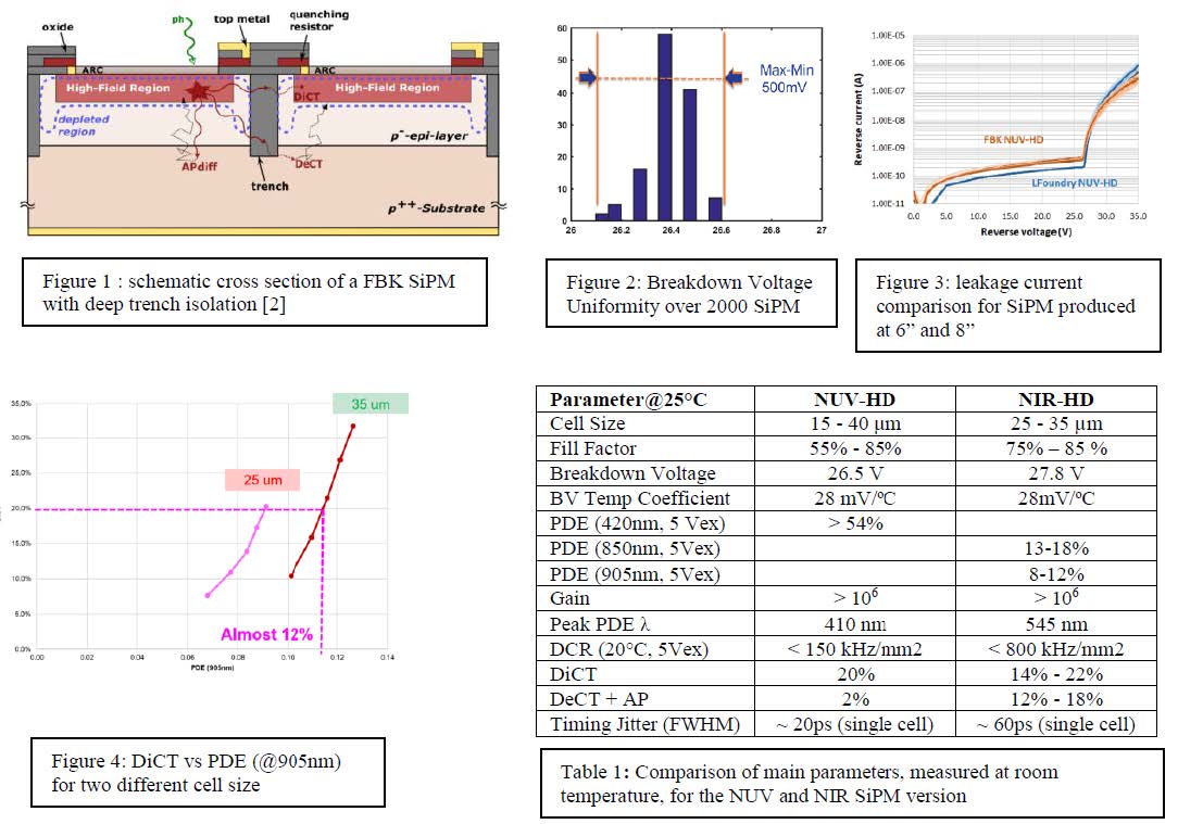
The FBK NUV-HD SiPM Technology [2], whose basic architecture is reported in Fig.1, has unique characteristics in terms of key parameters, as reported in Tab.1. These performances in the NUV spectrum, have attracted great interest from research institutes for large scientific experiments (like Darkside [4]). In order to satisfy the large volume required for such application, a technology transfer was done to LFoundry that has required the optimization and the re-engineering of several process steps. All the key parameters have been confirmed, demonstrating the intrinsic robustness of the chosen SiPM architecture and structure. Moreover, some behaviors have also been improved thanks to the integration into a fab already dedicated to a large volume production of optical sensors. Fig.2 shows the narrow distribution of the breakdown voltage, due to a more advanced process control. Also the leakage current has significantly decreased (Fig.3) due to the process steps already optimized for the reduction of the dark current into standard CMOS Image Sensors (CIS).
Such performances in a large volume manufacturing environment, have attracted electronic industries for large applications, especially in the medical field in the Near-UV range, but also in the automotive fields, requiring FBK and LFoundry to transfer also the NIR-HD technology optimized for the Near-IR range [4].
The process engineering capability at 8” will allow further optimization and development of SIPM with the introduction of dedicated module to further improve the performances, like, for example, the DiCT (Fig.4) and enlarge the working electromagnetic spectrum.
References
[1] Renker, D. Geiger-mode avalanche photodiodes, history, properties and problems. Nucl. Instrum. Meth. A 2006, 567, 48–56.
[2] A.Gola et al., Sensors 2019, 19, 308
[3] DarkSide Collaboration. “DarkSide-50 532-day Dark Matter Search with Low-Radioactivity Argon”. Physical Review D, 98 (2018): 102006. [ arXiv: 1802.07198 ]
[4] F.Acerbi et al., Nuclear Inst. And Methods in Physics Research, A, 912 (2018) 309-314