Choose timezone
Your profile timezone:
The 19th edition of the TREDI conference will be held in Torino, Italy.
The goal of the workshop is to bring together experts on sensor technology (design and processing), front-end electronics, system issues, detector applications (e.g., particle tracking, medical and biological imaging), etc., for discussions of the present state-of-the-art, establishment of requirements of the fields and future programs.
The workshop will include invited talks, contributed presentations and posters, and ample discussion time.
In the high-luminosity era of the Large Hadron Collider, the instantaneous luminosity is expected to reach unprecedented values, resulting in up to 200 proton-proton interactions in a typical bunch crossing. To cope with the resulting increase in occupancy, bandwidth and radiation damage, the ATLAS Inner Detector will be replaced by an all-silicon system, the Inner Tracker (ITk). The innermost part of the ITk will consist of a pixel detector, with an active area of about 13 m^2. To deal with the changing requirements in terms of radiation hardness, power dissipation and production yield, several silicon sensor technologies equipped with novel ASICs connecting by bump-bonding technique will be employed in the five barrel and endcap layers. As a timeline, it is facing to pre-production of components, sensor, building modules, mechanical structures and services.
This contribution presents the status of the ITk-pixel project focusing on the lessons learned and the biggest challenges towards production, from mechanics structures to sensors, and it will summarize the latest results on closest-to-real demonstrators built using module, electric and cooling services prototypes.
A beam telescope based on the Timepix4 ASIC was built in order to perform tests of synchronous multiple-detector readout and track reconstruction with fast timing capability.
The telescope consists of eight planes with n-on-p silicon sensors, each bump bonded to a Timepix4 ASIC. Four of these planes are instrumented with 300 µm thick planar sensors, and they are tilted with respect to the be incidence to provide high quality spatial measurements. The other four planes have 100 µm thick sensors to achieve a better time response.
The Timepix4 is designed to record both the time of arrival (ToA) and the time over threshold (ToT) for each discriminated signal. It has a 448 × 512 pixel matrix with square pixels at a 55 μm pitch. Each superpixel, a group of two by four pixels, has a 640 MHz voltage controlled oscillator (VCO). The VCO has four phase shifted copies, which results in a ToA digitisation with time bins of 195 ps. The ToT is proportional to the charge collected by the silicon sensor, and is used to improve spatial resolution based on charge sharing. The ToT is also used to correct for timewalk and improve the ToA resolution. After VCO and timewalk corrections the timing resolution of each plane improves significantly. The measurements can be combined to achieve a more precise time stamp on a track. In this presentation a detailed overview of the most recent results in temporal and spatial resolutions obtained by the telescope will be shown.
The High Luminosity program of the LHC collider (HL-LHC), expected to start in 2029, will provide almost a factor 5 increase in the instantaneous luminosity and a factor 10 in the integrated luminosity compared to the current LHC.
The HL-LHC poses unprecedented challenges to the inner tracking pixel-based systems: pixel hit rates up to 3 GHz/cm$^2$, hadron fluences exceeding 10$^{16}$ n$_{eq}$/cm$^2$, total ionizing dose up to 1 Grad, extended detector acceptance up to $|\eta|$=4.
This contribution will review the most relevant design and technological choices taken by the CMS collaboration for the upgrade of its Inner Tracker, along with the ongoing validation of the prototypes in preparation for large-scale production.
The CMS Precision Proton Spectrometer (PPS) was designed for measuring protons that escape along the LHC beam line after the interaction in CMS. It has successfully taken data during the LHC Run 2, collecting more than 110 fb-1 of integrated luminosity, and since 2022 is taking data in Run 3. A substantial upgrade of the PPS tracker was designed in preparation for Run 3, concerning the sensors, readout electronics, and detector mechanics. It employs new single-sided 150 um-thick silicon 3D pixel sensors, read out with the PROC600 chip used in the layer 1 of the CMS pixel tracker after the Phase 1 upgrade. An innovative mechanical solution was adopted to mitigate the radiation effects caused by the non-uniform irradiation of the readout chip, which were the main limiting factors in the Run 2 performance: miniaturised stepping-motors have been coupled with the detector mechanics, allowing for vertically moving the installed detectors during beam downtimes. In this contribution we will present the new apparatus installed for Run 3 and the preliminary performance results obtained by analysing the Run 3 data collected up to now.
The CMS experiment will be upgraded with a MIP Timing Detector (MTD) for the High-Luminosity phase of the LHC (HL-LHC). The precise timing provided by MTD will help mitigate the effects of the challenging pile-up conditions expected at the High-Luminosity LHC and extend the physics reach of the experiment. The Endcap Timing Layer (ETL) will instrument the forward region of the MTD detector, covering the pseudorapidity range 1.6 < |eta| < 3.
ETL will be made of Low-Gain Avalanche Diodes (LGADs) coupled to the Endcap Timing Read Out Chip (ETROC). The first batch of production LGADs is expected in 2025. This talk will present the plans for the Quality Assurance & Control (QAQC) of the LGADs at the vendor sites. I will discuss in detail the LGAD testing plans, describing measurement methods and the needed instrumentation, then I will report on the results obtained from the prototype LGADs (with an almost final design) used to validate the procedure.
The SIG and MERLINO INFN projects are developing new technologies for Particle Therapy beam monitoring systems, also integrating range a verification technique based on Prompt Gamma Timing (PGT) with a primary particle beam monitor able to track the single particles.
The aim of the final system is to measure on-line the time difference between a single primary particle crossing a thin silicon detector and the secondary prompt photons detected by a scintillation detector .
Materials and methods
Thin silicon detectors with and without gain layer and segmented in strips were used for the primary particle time measurement, and either one or seven cylindrical 1.5’ LaBr3(Ce) crystals were used for prompt photon time measurement. Different experimental setups were developed and tested at CNAO in Pavia (Italy), delivering proton beams of 227 MeV at sub-clinical rate (2-4E7 pps) as well as carbon ion beams of 398 MeV/u at both sub-clinical and clinical rates (5E7-E8 pps).
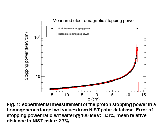
Aiming to reconstruct the proton stopping power, tests were performed irradiating a homogeneous PMMA phantom with a proton beam and detecting the secondary photons with a set of seven LaBr3(Ce) scintillators in different positions along the beam line readout. The time of primary protons was evaluated from the signals from 8 strips, 2 mm2 area each, of a LGAD sensor with 60 um thickness readout by an 8-channel custom frontend board. The signals from both detectors were acquired by means of a 2.5 Gs/s CAEN digitizer.
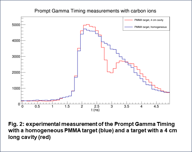
In tests with carbon ion beam at sub-clinical rate only one PMT and a strip silicon sensor without gain layer were used. First, a homogeneous PMMA phantom was irradiated, then a phantom with a 4 cm air cavity to evaluate the sensitivity of the PGT system .
Finally, to test PGT at clinical rate and with different carbon ion beam energies, a 2.7 x 2.7 cm2 silicon sensor hosted on a 144-channel frontend board based on ABACUS ASICSs was used. Only 8 digital outputs were readout through a CERN PicoTDC ASIC interfaced with a Virtex7 FPGA. This DAQ allows continuous acquisition, with a vast duty cycle improvement with respect to the digitizer-based acquisitions. The secondary photons emitted in a three-slab PMMA phantom were measured by a scintillator detector, readout by SiPMs matrices.
Results
The PGT distributions from tests with protons were processed with a Maximum Likelihood Expectation Maximization algorithm followed by a regression analysis, to reconstruct the proton stopping power in the homogeneous target (Fig. 1).
With the carbon ion beam at sub-clinical rate, the resulting PGT distributions with and without the 4-cm air cavity were clearly different and allowed us to identify the cavity (Fig.2).
The optimized DAQ for primary particles allowed us to precisely measure the beam particle time distribution and the bunch structure with an unprecedented detail level.
Conclusions
Non-invasive and real-time approaches such as PGT are desired to monitor therapy effectiveness and reduce uncertainties in treatment planning. First tests of a prototype of PGT system were successfully performed with both protons and carbon ions at sub-clinical and clinical rate.
A proof-of-principle setup with two bent silicon crystals is planned to be operated during LHC Run 3. It serves as preparation for an experiment aimed at measuring the dipole moments of charm baryons, from LHC Run 4 onwards, relying on the phenomena of particle channeling and spin precession in the bent crystals.
A silicon pixel module, based on the LHCb Velo sensors, is currently under construction for the proof-of-principle setup. Its task will be to measure the deflection of protons with energies in the TeV range that have been channeled in the bent crystals. The detector will operate in the secondary vacuum of a movable chamber (Roman Pot), which can be positioned inside the LHC's main vacuum.
This contribution discusses the design and integration of the detector module and Roman Pot, along with its expected performance.
The frontier activities of nuclear and subnuclear physics require devices with excellent performance in terms of stability and ability to operate at high fluxes of incident particles. Silicon carbide could be a good alternative to silicon devices due to its high resistance to radiation.
In this work we present the radiation damage study of a new, large area, p-n junction silicon carbide detectors. Several devices were irradiated in different experimental conditions to study their general performance as a function of fluence. Some detectors were collimated and irradiated with an oxygen beam, other devices instead were irradiated without collimation and with an aluminum beam. Both spectroscopies and electrical characteristics were investigated after the irradiation: the new detectors manifest excellent performance in terms of stability of the main parameters, linearity, defect distribution, charge collection efficiency, energy resolution, leakage current etc.
Moreover, a standard p-n junction silicon detector was also irradiated for comparison: SiC devices shown a radiation resistance more than two order of magnitude higher than Si devices.
Silicon Carbide (SiC) has gained attention in recent years for a number of benefits as a sensor material, especially its low leakage current in harsh radiation fields and at elevated temperatures. This study focuses on investigating intrinsic and radiation-induced defects in n-type 4H-SiC devices. The sensors studied were manufactured by IMB-CNM, with a 5µm or 50µm thick epitaxial layer on top of a 350µm thick 4H-SiC substrate. The samples were irradiated with 23GeV protons at the CERN IRRAD facility to 1E+11 to 1E+15 p/cm². TSC and DLTS measurements were performed in the temperature range of 20K to 350K. The presented results include IV and CV measurements taken before and after irradiation, as well as the defect parameters obtained from TSC and DLTS measurements.
Radiation damage significantly impacts the performance of silicon tracking detectors in Large Hadron Collider (LHC) experiments such as ATLAS and CMS, with signal reduction being the most critical effect. While adjusting sensor bias voltage and detection thresholds can help mitigate these effects, generating simulated data that accurately mirrors the performance evolution with the accumulation of luminosity, hence fluence, is crucial.
The ATLAS and CMS collaborations have developed and implemented algorithms to correct simulated Monte Carlo (MC) events for radiation damage effects, achieving impressive agreement between collision data and simulated events.
In preparation for the high-luminosity phase (HL-LHC), the demand for a faster ATLAS MC production algorithm becomes imperative due to escalating collision rates, events, tracks, and hits, imposing strict constraints on available computing resources. This talk outlines the philosophy behind the new algorithm, its implementation strategy, and the essential components involved. The presentation also includes results from closure tests and first evaluation of algorithm performance.
The next generation of high-energy and high-intensity hadron colliders for particle physics will require tracking detectors able to efficiently record charged particles in harsh radiation environments, where expected fluences exceed 10$^{17}$ particles/cm$^{2}$.
Recently, thin Low-Gain Avalanche Diodes (LGADs), with an active thickness of $\sim$ 50 $\mu m$, have proven their ability to combine precise timing with precise tracking measurements, making them suited candidates for 4D tracking in future experiments. At present, the gain mechanism of LGAD sensors under irradiation is maintained up to a fluence of 3$\cdot$10$^{15}$ particles/cm$^{2}$.
To enable the usage of LGADs in the extreme fluence regime, an innovative design of the LGAD gain layer, the p$^{+}$ implant responsible for the local and controlled signal multiplication has been implemented to enhance their radiation tolerance by more than one order of magnitude: the compensated LGAD.
In the standard LGAD design, the gain layer is obtained by implanting a high dose of an acceptor dopant, referred to as p$^{+}$, in the region below the n$^{++}$ electrode. In the compensated design, the gain layer results from the overlap of a p$^{+}$ and an n$^{+}$ implant: the difference between acceptor and donor doping will bring an effective concentration similar to standard LGADs. The new design will be more resilient to radiation, as both acceptor and donor atoms will undergo removal with irradiation, but if properly engineered, their difference will remain constant. Therefore, the compensated LGADs will empower the 4D tracking ability to a fluence of 10$^{17}$ particles/cm$^{2}$ and above.
The first production of compensated LGAD sensors has been released by the FBK foundry at the end of 2022. Electrical characterisation and signal analysis from compensated LGAD sensors before and after irradiation with neutrons will be presented and discussed. Future evolution of the design of compensated LGADs will be envisaged.
The dual-radiator (dRICH) detector of the ePIC experiment at the future Electron-Ion Collider (EIC) will make use of a large array of silicon photomultipliers (SiPM) sensors for the detection of the emitted Cherenkov light. The photodetector surface will cover ~ 3 m2 with 3x3 mm2 pixels, for a total of more than 300 k readout channels. SiPM is the emerging solid-state technology for photon detection and the application of SiPM for RICH at the EIC will be the first use of SiPM for single-photon detection in a HEP experiment. SiPMs show significant advantages when compared to vacuum-based photodetector technologies, owing to their high photon detection efficiency also in high-magnetic field environments. This is a top asset for the ePIC experiment at the EIC, where the magnetic field at the location of the dRICH photodetector surface is high (~ 1 T). It is on the other hand known that SiPMs are sensitive to radiation damage and require rigorous testing to ensure that their single-photon counting capabilities and dark count rates (DCR) are kept under control over the years of running of the ePIC experiment. The DCR can be maintained to an acceptable rate, below ~ 100 kHz/mm2 as required for this application, by reducing the SiPM operating temperature and by recovering the radiation damage with high-temperature annealing cycles. Moreover, the background from the sensor DCR can be reduced by using the excellent SiPM timing capabilities coupling it with high-precision fast TDC electronics.
In this talk we present an overview of the current status of the R&D and the results of studies performed on significant samples of commercial and prototype SiPM sensors. The devices have undergone proton and neutron irradiations aimed at studying the device performance with increasing non-ionising energy loss (NIEL) doses up to 1011 1-MeV neq/cm2, the device recovery with long high-temperature annealing cycles and the reproducibility of the performance in repeated irradiation-annealing cycles. We studied the use of the self-heating capabilities of the SiPM to exploit the Joule effect as a potential effective way to perform the high-temperature annealing "in-situ". We also report on the results obtained from two beam tests performed in October 2022 and in October 2023, where the SiPM sensors were mounted on the optical plane of the dRICH detector prototype and successfully recorded Cherenkov photon rings at the CERN PS accelerator. The data have been collected with a complete chain of front-end and readout electronics based on the first 32-channel prototypes of the ALCOR chip, a newly designed ASIC for SiPM readout.
The FASER experiment at the Large Hadron Collider (LHC) aims to detect new, long-lived fundamental particles and to study neutrino interactions. To enhance its discovery potential, a W-Si preshower detector is being built, targeting surface commissioning and then installation during the second half of 2024. The new preshower will enable the identification and reconstruction of electromagnetic showers produced by high-energy photon pairs with separations as fine as 200 µm. The detector incorporates a cutting-edge monolithic ASIC with hexagonal pixels measuring 100 µm in pitch, designed to achieve an extended dynamic range for charge measurement and capable of storing charge information for thousands of pixels per event. The ASIC integrates fast front-end electronics based on SiGe heterojunction bipolar transistor technology, providing a O(100) ps time resolution. Analog memories embedded within the pixel array facilitate frame-based event readout, minimizing dead areas. In this presentation, we detail the design and expected performance of the preshower detector, along with the results from lab characterisation of pre-production ASIC prototypes, and of the first module prototypes.
In this contribution, we will present the very preliminary experimental performances obtained with the ASIC FAST3. FAST3 is a multi-channel amplifier optimized to read out LGAD sensors and designed to achieve a temporal jitter below 20 ps.
FAST3 was developed by the microelectronic group of INFN Turin. FAST3 has been designed in UMC 110 nm CMOS technology, and has 16 channels distributed over a surface of 1x5 mm2; the power rail is 1.2 V and the expected power consumption is 2.4 mW/ch. Each FAST3 readout channel presents an amplifier with low input impedance (<50 Ohm), and wide bandwidth (~ 1 GHz) and wide input range in terms of charge (3-40 fC).
The experimental tests presented include i) charge injection through an external pulser, in order to evaluate the temporal jitter of the ASIC as a function of the injected charge; ii) the characterization of the temporal performances of the ASIC coupled with an LGAD sensor 50µm thick, using a Sr90 beta source to generate non-uniform signals inside the LGAD.
The design of the Micro Vertex Detector (MVD) for the PANDA experiment is optimized for the detection of secondary vertices and maximum acceptance close to the interaction point. The MVD consists of a 4-layer barrel section, placed around the interaction point, and a 6-disks forward section, located in the forward position. The outermost layers of the MVD will be equipped with double sided Silicon Strip Detectors (SSDs).
The SSD electronic readout must provide both the spatial position and the energy deposited by the impinging particles. Moreover, since PANDA is a triggerless experiment, each event must be tagged with its time of arrival (ToA). In order to cope with these requirements a 64-channel dedicated ASIC, named ToASt, has been designed and tested. Each channel includes a charge-sensitive amplifier, a current mode shaper, a linear time over threshold (ToT) stage and double threshold discrimination. A 12-bit time stamp is distributed to all channels; its value at the two edges of the output comparator is stored, thus providing both ToA and ToT. The two values are immediately readout by a digital interface, formatted in 32-bit words and transmitted via two 160 MS/s serial links.
ToASt is designed in a commercial 110 nm CMOS technology. The die size is 4.4$\times$3.2 mm$^2$; the input pads are located on one side of the die while all other pads are on the opposite side, thus allowing multiple dies being placed very close to each other. The digital logic has been triplicated for Single-Event Upset (SEU) protection.
ToASt has been extensively tested in laboratory standalone and connected to a detector, showing excellent performances. It has also been used in a beam test at the COSY facility in Juelich. Radiation tolerance tests for total dose and SEU have also been performed.
ASTRA-64 (Adaptable Silicon sTrip Read-out ASIC) is a 64-channel mixed-signal custom IC designed for micro-strip silicon sensors read-out. Manufactured in a 110-nm technology node, it comprises two identical mirrored subcircuits, each accommodating 32 channels.
Recursively, each channel integrates two main blocks: a charge-sensitive amplifier and a shaper. The former features two programmable gain settings suitable for positive and negative input polarities, whereas the latter provides four adjustable peaking time. The overall gain is calibrated to provide linear charge measurements of up to 160 fC and 80 fC – depending on the amplifier settings – optimizing the noise performance based on the detector capacitance.
ASTRA-64 offers two distinct read-out modes. In the analog one, sampled voltages are sent off-chip via an analog multiplexer linked with a differential output buffer. Conversely, the digital read-out mode employs a Wilkinson ADC for each channel to digitize voltage and a shared serializer to transmit data via an SLVS driver. Additionally, ASTRA-64 embeds a fast shaper and a leading-edge hysteresis discriminator per channel to produce rapid trigger signals. A FAST-OR logic merges these signals to provide a single off-chip trigger.
The IC first application is the Silicon Charge Detector of the HERD experiment – slated for installation aboard the Chinese space station in 2027 – to implement tracking and supplementary charge measurements. The space application adds the necessity to comply to its stringent requirements, primarily with a power-dissipation limit of 600 µW per channel.
In this work we will present the tests, characterization, and performance of ASTRA-64, mainly focusing on its charge linear input range and resolution.
Particle detectors at future lepton or hadron colliders will require covering a very large area with a tracker with fine spatial resolution of O(10)um. A timing capability of O(10)ps in addition should improve the tracking reconstruction, particle identification of charged particles and mass measurement of newly discovered particle. Capacitive-coupled Low-Gain Avalanche Diode (AC-LGAD) is a semiconductor tracking detector with precise timing resolution and spatial resolution developed by KEK and Tsukuba group collaborating with Hamamatsu Photonics K.K. (HPK). In this presentation we will focus about recent status of the development of AC-LGAD detector and possibility of improvement for timing resolution and radiation tolerance.
This contribution reports on the spatial and temporal resolutions of an RSD 450-micron pitch pixels array measured at the DESY test beam facility. RSDs, Resistive Silicon Detectors, also known as AC-LGAD, achieve excellent position and temporal resolution by exploiting charge sharing among neighboring electrodes. The RSD matrix used in this study is part of the second FBK RSD production, RSD2, and it is composed of 450~microns pitch pixel with cross-shaped electrodes. A 7-pixel matrix was read out by the FAST2 ASIC, a 16-channel amplifier fully custom ASIC developed by INFN Torino using the 110 nm CMOS technology. The position resolution reached in this test is 15 microns, about 3.4\% of the pitch. The temporal resolution achieved in this work is about 60 ps, dominated by the FAST2 resolution.
In this work, we present a detailed study of the spatial and temporal resolution of Resistive Silicon Detectors (RSD) with cross-shaped electrodes, measured using a high-energy protons/pions beam at CERN SPS, within the AIDAINNOVA collaboration. The tested RSD2 sensors, fabricated by FBK, have relatively large pixel sizes (1300 and 450 microns pitch) and innovative read-out electrode layouts geared toward reaching a uniform response over the whole surface.
The sensors performance was measured by reconstructing the tracks of 120 GeV pions/protons impinging on the devices, using the MIMOSA tracker and the Corryvreckan software package. The employed electronics is a low-noise discrete readout board specifically developed for LGAD testing: the Chubut2.
The results of such measurements yield excellent position resolution, about 20 µm for the 450 microns-pitch sensor, and time resolution typical of the LGAD technology. We will present a comparison with the resolutions obtained in the laboratory using the TCT setup, that highlights the various contributions to the temporal resolution.
Low Gain Avalanche Detectors for the ATLAS High Granularity Timing Detector: laboratory and test beam Campaigns
The High Granularity Timing Detector (HGTD) is designed for the mitigation of pile-up effects in the ATLAS forward region and for bunch per bunch luminosity measurements. HGTD, based on Low Gain Avalanche Detector (LGAD) technology and covering the pseudorapidity region between 2.4 and 4.0, will provide high precision timing information to distinguish between collisions occurring close in space but well-separated in time. Apart from being radiation resistant, LGAD sensors should deliver 35 ps time resolution per track for a minimum-ionising particle (40 ps per hit) at the start of lifetime, increasing to 50 ps per track (70 ps per hit) at the end of HL-LHC operation. Each readout cell has a transverse size of 1.3×1.3 mm2 leading to a highly granular detector with about 3 millions of readout electronics channels. A dedicated ASIC for the HGTD detector, ALTIROC, is being developed in several phases producing prototype versions of 2×2, 5×5 and 15×15 channels. HGTD modules are hybrids of the LGAD and ALTIROC connected through flip-chip bump bonding process.
Several test beam campaigns have been conducted at DESY and CERN SPS H6 beamline in 2022. The performance of irradiated Carbon-enriched LGAD sensors from different vendors has been studied. This talk covers the promising results in terms of collected charge, time resolution and hit efficiency of LGADs. A time resolution of < 70 ps is observed in most cases for highly irradiated sensors (2.5e15 neq/cm^2), while integrating timing information to the EUDET system allows for a surface resolution of less than 50 μm. First module prototypes of 15×15 arrays with a pad size of 1.3×1.3 mm2 for the HGTD project have been tested from different manufacturers. Their performance with charged-particle beams before irradiation is evaluated. The triggering architecture, picosecond synchronisation scheme and analysis logic will also be presented as well as application-specific electronics and components. A summary of the results from LGAD-only and hybrids will be presented.
L2
FBK has produced the Trench-Isolated LGADs (TI-LGADs) to study the effect of Carbon on breakdown and demonstrate the scalability of the technology for larger sensors. TI-LGADs have the potential to significantly reduce the no-gain region as compared to the standard LGAD technology. This contribution presents the electrical characterization of TI-LGADs produced under AIDA-INNOVA. The devices used for this study consist of 169$\times$168, 32$\times$32, 5$\times$5, and 2$\times$1 pixel sensors, and the measurements include the IV characteristics and yield. The results of this study provide a comparison between different layout designs and show how the number and width of trenches affect the breakdown of the sensors.
We present results obtained on the characterization of AC-LGAD sensors developed by Brookhaven National Laboratory (BNL), and TI-LGAD developed at FBK. These two technologies are promising candidates to achieve 4D charged particle tracking. In addition to tests with laser TCT, these devices have been investigated during a test beam campaign organized in the framework of the AIDAInnova WP6 project.
Space and timing resolutions were extracted for both technologies, together with the particle hit efficiency. In the case of the TI-LGAD, also the inter-pixel distance has been evaluated with test-beam data, and compared with previous laboratory measurements.
In this report we present the latest results from our comprehensive study on Ti-LGAD interpixel region under low and high charge injection, using fs-laser and SPA-TCT and TPA-TCT experimental techniques at ELI Beamlines, ELI ERIC. Samples have been investigated using probe station at the Institute of Physics of the Czech Academy of Science, and IV/CV distributions will be presented. All samples exhibit very strong ghost signals not synchronized with laser pulses and beside normal IP signal we recorded an extraordinary strong signal synchronized with normal IP signal produced by laser in IP region. Pixels are not affected by ghosts. No strong signal was observed in pad region.
Scanning at different depths using TPA and across the pad and interpixel region revealed the most sensitive region to the highest occurrence rate of the strong signals. Moreover, the dependence of signal characteristics on bias voltage and laser power at different temperatures is explored and tentative explanations for the observed behavior are offered. Furthermore, the occurrence rate of ghost signals with laser switched off and occurrence rate of strong signals vs shooting position of laser were systematically studied. The bias threshold for ghosts and laser pulse energy threshold vs bias for strong IP signals are viewed too.
Beside conventional way of presenting experimental data we recorded some videos to give better insight how the sensors behaves under TPA. and to show evolution of the signals (normal, strong, and ghosts) when scanned through the sensor (Z depth scan). Scans are done in 3 positions. pad, center of the IP and trench position. Interpixel region was also microscopically inspected.
In the last few years, Low Gain Avalanche Detectors (LGAD) have demonstrated their outstanding performance when detecting high-energy charged particles. However, the very nature of electrons and holes under avalanche multiplication highlights that this good performance is diminished when they are to detect low penetrating particles (e.g. low-energy protons or soft x-rays). A novel design of an LGAD detector, the nLGAD, was designed and fabricated at CNM in order to try to overcome this drawback. A qualitative description of the NLGAD concept is presented in this work, along with gain response measurements under UV light of 369 nm, visible light of 404 nm and IR light of 1064 nm; all of them carried out on test devices of the last IMB-CNM nLGAD fabrication batch. The results demonstrate the potential of the nLGAD for experiments that imply the detection of low penetrating particles.
Single photon counting and charge integrating hybrid pixel detectors are an established standard for photon science applications at hard X-ray energies between $\sim\,$2 keV and 20 keV. Their capabilities for high frame rates and dynamic range, large area coverage, high signal-to-noise ratio and spatial resolution also make them attractive for applications at soft X-ray energies (< 2keV). However, using hybrid detectors for soft X-ray detection has been difficult so far. This is mainly due to the low quantum efficiency of standard silicon sensors at soft X-ray energies and the noise of the readout electronics.
At PSI, we have been developing inverse Low Gain Avalanche Diode (iLGAD) sensors for soft X-ray detection in collaboration with FBK. These sensors feature an optimized thin entrance window, enabling a quantum efficiency at soft X-ray energies comparable to standard CCD and CMOS image sensors (i.e., 62% at 250 eV). The internal signal amplification in the iLGAD sensor improves the signal-to-noise ratio at low photon energies and enables single photon resolution down to $\sim\,$200 eV
We present the development of iLGAD-based hybrid detectors for soft X-ray photon science at PSI and illustrate the capabilities and current limitations of the technology. We discuss in depth characterization results of a prototype consisting of an iLGAD sensor bump bonded to the charge integrating 75 µm pixel JUNGFRAU chip. Cooled to -22°C, this system achieves an effective equivalent noise charge of ≤ 5.5 electrons r.m.s. at a 5 μs integration time. Single photon resolution at 200 eV with a signal-to-noise ratio better than 5 becomes feasible by cooling further to -50°C. Based on these results, we give an outlook on future improvements and show a first look on applications of iLGAD hybrid detectors for soft X-ray experiments.
Solid-state systems based on Si-microstrip sensors are a consolidated technology for precision particle tracking in space, as first demonstrated by the operations of the AMS-01 detector and confirmed by PAMELA, Fermi-LAT, AGILE, AMS-02, DAMPE. The next generation of large acceptance AstroParticle space detectors (e-ASTROGAM, AMEGO, PANGU, HERD, ALADInO, AMS-100) requires larger surface coverages with Si detectors. Si microstrip detectors are the most suitable solution to instrument such detectors, featuring a larger number of electronics channels, while coping with the limitations on power consumption in space.
In this talk we’ll review the state of the art of the tracking systems in space and of the sensors technologies currently used in active or near future experiments, and the potential technological improvements that can be investigated, developed and adopted for the next generations of large acceptance AstroParticle space detectors.
SiPM have proven to be a successful technology where fast single-photon counting is required. Although their application is mainly focused on visible/near IR detection, there is an active interest in extending SiPM sensitivity to vacuum UV (VUV). In fact, next generation rare event searches would greatly benefit from a VUV single photon sensitive device as it can guarantee higher radiopurity compared to PMTs. Efforts on maximizing the SiPM sensitivity in the VUV region developed a custom-designed manufacturing process that reaches a photon detection efficiency over 25%, meeting and exceeding requirements from experiments. Moreover, the R&D on through-silicon vias (TSV) enables efficient device/chip integration, allowing a compact and scalable photosensitive region to be deployed in a large cryogenic environment such as the one needed for rare event searches. With this poster the author reports the work performed at FBK on the design and test of VUV sensitive SiPMs equipped with TSV.
DarkSide-20k is the next future experimental project, that combines the
special technique for the procurement and purification of underground
Argon with the light detection technology based on large arrays of
customized cryogenic photosensors. Together with an accurate selection of
radiopure materials DS-20k experiment is expected to hunt for WIMPs in a
free background mode for an exposure > 100 tonne × year. A large dual
phase Time Projection Chamber surrounded by an active neutron veto based
on a Gd-loaded acrylic shell will be installed inside a cryostat membrane
under construction in the LNGS underground site and containing more than
700 t of liquid Argon. The two TPC optical planes will be instrumented
with more than 21 m2 of Silicon Photomultipliers arranged in 528 Photo
Detection Units that will be massively assembled in the Nuova Officina
Assergi (NOA) a large clean room of 420 m2 deserving cutting edge
technology equipments and in operation since the beginning of 2023. After
a short introduction on Darkside-20k and the PDU concept design, the main
features of NOA clean room packaging site and all the steps of the PDU
production workflow will be presented.
Silicon Photomultipliers (SiPMs) have gathered interest in several fields from High Energy Physics experiments to biomedical applications thanks to their excellent energy and timing resolution, together with their low operating voltage, low cost, ruggedness and insensitivity to the magnetic fields. The modeling of the SiPM in terms of equivalent electrical circuit and the estimation of its electrical parameters are fundamental to properly simulate the device response for a proper front-end design and possibly tailor the sensor to match the requirements of the research experiments. Many efforts have been made in order to create a general and reliable equivalent electrical model and to simulate the SiPM response. Moreover, in the last years, excellent results in terms of timing performance have been achieved thanks to the improvement of the scintillator crystal materials, the electronics readout and the detector development. In this work we focused on the simulation of a single microcell (SPAD) and on the timing performance in terms of Single Photon Time Resolution (SPTR) of the recently introduced FBK NUV-HD Metal in Trench (MT) technology.
An improved SPICE simulation has been implemented by using a new model for the diode capacitance $C_d$. This is typically considered constant whereas in some SiPM technologies it has been found to change with the applied excess bias. The reliability of the model has been confirmed by extracting the electrical parameters of the SPAD at different excess bias and comparing the simulated and the measured overall single-cell response.
The SPTR measurement has been performed by using a femto-second laser with a wavelength of $390nm$ and by testing SPADs with different microcell sizes and different layout versions: with or without a metal mask outside the active area (capacitive coupling). Moreover, a $1mm\times1mm$ and a $3mm\times3mm$ SiPMs with $40\mu m$ cell size and M0 masking version have been tested. By using a high frequency readout electronics, we achieved an outstanding SPTR of about $\simeq 19ps$ and $\simeq 30ps$ FWHM for the SPAD and $1mm\times1mm$ SiPM with $40\mu m$ M0 masking respectively.
We found that the single cell response simulated with the new model matches the experimental acquired signal with a discrepancy below 5%, which is a significant improvement with respect of the constant capacitance model. Moreover, further investigations will allow to understand the role of the metal masking in the timing performance and to discuss about limitations and future improvements.
Over the last few years, Fondazione Bruno Kessler (FBK, Trento, Italy) has gained experience in the development of several Silicon Photomultiplier (SiPMs) technologies. The SiPM is a solid-state photodetector, sensitive to single-photons, which is becoming the device of choice in different applications, ranging from the big physics experiments to medical applications, such as time-of-flight positron emission tomography (TOF-PET), in which a fast timing is a strong requirement.
Following this direction, FBK is developing a new SiPM technology, called Near-Ultraviolet Sensitive deep-junction (NUV-DJ). The development is being carried out using an external silicon foundry. The NUV-DJ microcell (SPAD, Single Photon Avalanche Diode) is based on a p-type, high-resistivity, epitaxial layer, grown on top of a low-resistivity n-type bulk. Conversely to traditional FBK SiPMs, the high-electric field region is located deeper in the device. This allows electrons to trigger the avalanche also when the carriers are photogenerated deeper below the surface by longer wavelength photons, thus enhancing the avalanche triggering probability.
In the first production, several 8-inch wafers were manufactured, and the main process and layout split were tested. We carried out an extensive characterization, including the current-voltage characteristic, photon detection efficiency (PDE), the primary noise rate, single photon time resolution (SPTR), and coincidence time resolution (CTR) using LYSO scintillators. The measured breakdown voltage in all the wafers was aligned with the expected values from the TCAD simulations. The best layout and process split showed a maximum excess bias (limited by the so-called second divergence of the correlated noise) larger than 20 V, confirming the effectiveness of the new SPAD structure and the good optical isolation between microcells. The PDE showed unprecedented values of 70% (including a nominal fill factor of 80.8%), at 420 nm of wavelength and 10 V of excess bias. Moreover, we measured a SPTR of 60 ps FWHM at 20 V of excess bias, for a 4x4 mm$^2$ SiPM and a CTR of less than 100 ps FWHM using a 2.76x2.76x18 mm$^3$ LYSO:Ce crystal at 10 V of excess bias.
These results are state-of-art as regards timing and PDE, thus very interesting for TOF-PET applications using either LYSO, LSO, BGO, LaBr3 crystals or in an experiment where a high PDE in the NUV region is a requirement.
The LHCb experiment at CERN is preparing a major upgrade to cope with the increase of instantaneous luminosity at LHC scheduled for Run 5. LHCb detector will operate at an instantaneous luminosity of about $1.5 \times 10^{34} \, cm^{-2} \, s^{-1}$. In these conditions approximately 2000 tracks from 40 proton-proton collisions will cross the vertex detector every $25 \, ns$.
To properly reconstruct primary and secondary vertices, the development of sensors and electronics capable of measuring the particle hit time with an accuracy of $50 \, ps$ and a spatial resolution of 10 µm is crucial, in order to maintain the current vertex reconstruction efficiency also at high luminosity. 3D trench silicon pixels, developed by the INFN TimeSPOT collaboration, is a technology aiming to fulfill these requirements. These $150 \, µm$ active thickness, $55 \, µm \times 55 \, µm$ silicon pixels, consisting of $40 \, µm$-long planar trench electrodes located between two continuous bias electrodes, provide a time resolution of about $10 \, ps$ and $99\%$ detection efficiency for minimum ionizing particle detection. The increase of the instantaneous luminosity will require detectors able to withstand the increased radiation damage.
For this reason, sensors irradiated at different radiation levels (from $10^{16}$ and up to $10^{17} 1\, MeV \, n_{eq} \, cm^{-2}$) are being tested.
Preliminary results, that will be presented at the conference, show that 3D trench-type silicon sensors are proving to be a very promising candidate for future vertex detectors.
The ATLAS Inner Detector will be completely replaced with an all-silicon Inner Tracker (ITk) to withstand the harsh operational conditions of the High Luminosity LHC at CERN. The ITk pixel detector will be located in the innermost part of the tracker. It will be instrumented with different sensor technologies, 3D and planars, according to the expected total fluence, which reaches up to 1.9·1016 neq/cm2 (safety factor of 1.5 included), and the required performance.
Pixel sensors with 3D technology will instrument the innermost layer (L0), with pixel size of 50×50 μm2 in the endcap and 25×100 μm2 in the barrel. A large effort to study the variety of pre-production pixel detectors, designed and produced by FBK and Sintef is ongoing. An overview of the results is presented, with particular focus on test beams campaigns.
In the talk, ongoing activities on 3D processes will be presented. FBK is actively involved in the realization of detectors with RD53 and CROC designs for both ATLAS and CMS experiments. The latest developments and parametric measurements with Temporary Metal for these processes will be discussed. Additionally, FBK is continuing the development of 3D sensors based on trenches. Due to their geometry, these sensors are considered candidates for achieving excellent temporal resolutions along with high damage resistance. In the AIDA Innova project, FBK is producing a batch, and the main characteristics of this batch will be highlighted.
The MONOLITH H2020 ERC Advanced project aims at producing a high-granularity monolithic silicon pixel detector with picosecond-level time stamping. Such extreme timing exploits fast and low-noise SiGe BiCMOS electronics, and a novel sensor concept: the Picosecond Avalanche Detector (PicoAD).
A prototype without internal gain layer and 100µm pixel pitch was produced in 2022.
Lab measurements with a femtosecond laser provided time resolutions down to 2.5 ps. Testbeam measurements showed full efficiency and 20 ps time resolution at a power consumption of 1 W/cm^2 and a sensor bias voltage HV = 200 V. This prototype after being irradiated up to 1x10^16 neq/cm2, still provides an efficiency of 99.7% and 45 ps at HV = 300 V.
The novel PicoAD sensor uses a patented multi-PN junction to engineer the electric field and produce a continuous gain layer deep in the sensor volume. The result is an ultra-fast current signal with low intrinsic jitter in a full fill factor sensor. A proof-of-concept monolithic PicoAD demonstrator provided full efficiency and 13 ps at the center of the pixel, while the time resolution raised to 25 ps in the inter-pixel region. The first batch of PicoAD prototypes with different geometries and gain-layer implant doses was delivered in January 2024; preliminary results will be shown.
The 100 µPET project is developing a novel small-animal PET scanner for ultra-high-resolution molecular imaging. The design consists of four towers surrounding the tissue to be analysed, each containing 60 layers of monolithic pixel sensors and flexible printed circuits.
The monolithic pixel sensor based on SiGe BiCMOS technology with HBTs offers high bandwidth and efficient noise-power trade-off. The 2.3 cm x 3.0 cm ASIC integrates a matrix of 132 x 192 hexagonal pixels with a pixel area of (150 µm)², which allows for an extremely low volumetric granularity.
The read-out architecture is designed to handle an event rate of 10 kHz/cm², with each event consisting of a single cluster of up to 5x5 pixels. A high efficiency with a low fake hit rate can be achieved with a pixel threshold of 3000 e-, an ENC of 200 e- and a 3-bit DAC for pixel-level threshold tuning. The binary event-driven read-out provides the pixel address encoding on a fast bus, while a fast-or signal is sent to a periphery TDC for time-of-arrival and Time-Over-Threshold measurements. A system-level time resolution of 200 ps is achieved within a power budget of 100 mW/cm². The precise timing information is crucial for selecting true coincidence events and enhancing image quality in single-event imaging applications.
The design of the monolithic pixel sensor and scanner system along with simulation results will be presented.
The RD50-MPW chip series are generic R&D High Voltage CMOS pixel chips aimed at boosting the performance of this sensor technology especially in terms of radiation tolerance, timing resolution and pixel size in view of the harsh requirements imposed by future physics experiments on tracking systems. The latest prototype, RD50-MPW4, demonstrates significant improvements on the current-to-voltage characteristics and pixel noise suppression with respect to its predecessor, RD50-MPW3. To achieve the current-to-voltage characteristics improvements, RD50-MPW4 uses floating p-stop style pixel-to-pixel isolation, implements an optimised multi-guard ring around the chip and has been backside processed to enable backside substrate biasing. The pixel noise suppression is the result of the strategic separation of the power and ground domains between the pixel matrix and peripheral digital readout.
RD50-MPW4 features a 64 rows x 64 columns matrix of 62 µm x 62 µm pixels with both analogue and column drain digital readout electronics embedded inside the large collection electrode. The pixel electronics incorporate logic to mask noisy pixels and an 8-bit SRAM shift register for serial configuration. RD50-MPW4 implements a double column scheme, which together with the 8-bit SRAM shift register, alleviates the routing congestion and facilitates means to minimise the crosstalk. The prototype has an advanced digital periphery for effective pixel configuration and fast data transmission, which consists of one end of column circuit per double column and a slow control system based on the I2C protocol for external communication using an internal Wishbone bus. The event data generated by the pixels is packed into frames, zero suppressed and encoded following the 8b/10b Aurora protocol. It is serialised over a single 640 Mb/s LVDS line. The RD50-MPW chip series are in the 150 nm High Voltage CMOS process from LFoundry S.r.l.
This contribution will focus on the design of RD50-MPW4 and its preliminary evaluation results.
M2
Monolithic CMOS silicon sensors represent an important innovation for high-energy physics experiments due to their cheaper production and assembly cost compared to hybrid ones. Indeed, in hybrid devices, the electronics and the sensor are produced in different silicon substrates which must be later connected using bonding techniques. However, as far as the time resolution is concerned, the most mature and high-performance technology today is the Low Gain Avalanche Diode one (LGAD), where a silicon sensor with an internal gain is connected to a custom electronics in a hybrid way.
The recent developments exploit the integration of the LGAD concept in CMOS Monolithic Active Pixel Sensors (MAPS) to obtain the benefits provided by both technologies. The multiplication of the signals in MAPS has a major impact on the signal-to-noise ratio, hence the power consumption of the in-pixel front-end can be lowered to achieve the same performances. In addition, this feature increases the attractiveness of these devices for space applications where low power absorption is desired. Nevertheless, the union of the two technologies still lies in its early stages and a vigorous R&D is necessary.
This presentation will focus on the structures with internal gain fabricated in a standard 110nm CMOS technology for the third run of the ARCADIA project. An overview on the recently produced passive structures will be provided together with the results obtained in the laboratory. Then, a description of the first prototype with integrated electronics will follow along with its characterisation. Measurements obtained using an infrared laser and a Sr90 radioactive source will be presented. Finally, the future perspectives of the next steps and an insight into the ongoing R&D will be given.
The ITS3 project foresees the use of ultra-light monolithic active pixel sensors (MAPS) for the vertex detector in the ALICE experiment at the LHC to drastically improve the performance of the ALICE tracking and vertexing system. The MAPS are produced in a 65 nm CMOS process in large, 12-inch wafers. Stitching allows the fabrication of wafer-scale sensors that can be thinned to around 50 µm and bent to form half-cylindrical detection layers.
This contribution discusses the analogue pixel test structure (APTS) produced in 65 nm. The APTS is used to understand the analogue properties of the TPSCo 65 nm technology and to compare the charge collection performance in different processes and pitches. Recent results from lab and test beam characterisation are presented, showing that a hit efficiency of more than 99% is achieved for all collection electrode geometries before and after irradiation up to 1e14 1 MeV n_eq. In-pixel studies show the dependence of the efficiency on the position inside the pixel cell. The achievable spatial resolution of less than 3 µm for pixel pitches of 10 µm. Finally, the applicability of 65 nm MAPS for FCC-ee vertex detectors that feature similar requirements as ALICE ITS3 will be discussed shortly.
Hybrid Pixel Detectors (HPDs) have been widely adopted for diffraction-based modalities in electron microscopy thanks to their high frame rates (> 1 kHz) and large dynamic range. However, they are less suitable for imaging applications because of their poor spatial resolution due to relatively large pixels (≥ 25 μm) and to the multiple scattering of high-energy electrons (> 100 keV) in the thick sensor layer. For cryogenic electron microscopy (cryo-EM) the state-of-the-art are thin monolithic CMOS devices with small pixels (≤ 15 μm pitch). To fully realize the potential benefits of fast, radiation hard HPDs for all modalities of electron microscopy, we are developing deep learning methods to reconstruct the impact points of incident electrons for the 25 μm MÖNCH pixel detector [1]. Exploiting the small pixels to track the electrons and using deep learning to obtain subpixel resolution, we aim to extend the use of HPDs to cryo-EM imaging and develop a detector for both diffraction and imaging applications.
We have developed several deep learning models to localize the electron impact point based on both simulations and measured data, extending the work presented in [2, 3], which was based on only synthetic data. Simulation samples are obtained using Geant4-Medpix [4]. For the measurement-based training, we have focused the electron beam to a sub-pixel region to label tracks with ground truth impact points. A sub-pixel spatial resolution has been achieved for 200 keV electrons. We will show details of the deep learning model design, training scheme, and evaluation results. Example images of some standard samples will also be presented, in addition to the detective quantum efficiency measurements, to act as a benchmark of the system’s abilities. Lastly, the data processing pipeline for the MÖNCH detector for its use in electron microscopy will be discussed.
[1] M. Ramilli et al., JINST 12 (2017) C01071
[2] J. Paul van Schayck et al., Ultramicroscopy, 218 (2020), 113091
[3] B. Eckert et al., IEEE Transactions on Nuclear Science, 69 (2022), 1014-1021
[4] A. Schübel et al., JINST 9 (2014) C12018
Sim1
Future high-energy physics experiments will consider measuring concurrently the location and the time of a particle hit with very good accuracy, i.e., 4D trackers should be the basic option for future detection systems.
Within this framework, DC-coupled Resistive Silicon Detectors (DC-RSD), an evolution of the AC-coupled design, are considered a very promising option. They combine two different design innovations, Low-Gain Avalanche Diode (LGAD) and resistive readout (RSD), to achieve a spatial resolution of a few micrometres using large pixels (150-200 μm), providing an excellent time resolution (~30 ps).
The concept of DC-RSD has been finalised using an innovative mixed-mode approach to simulation: SPICE-based fast modelling to derive the sensor design parameters, followed by full 3D TCAD simulations of the sensor behaviour. In particular, TCAD simulations have been an excellent tool not only to understand the sensor operation, but also to design and optimise this innovative class of detectors. This involved the evaluation of different technology options (e.g., the resistivity of the n+ layer, contact materials) and geometrical layouts (shape and distance of the readout pads), aiming to obtain a better control on signal spreading, and thus the use of DC-RSD sensors in high-occupancy applications.
This contribution reports the latest TCAD simulation outcomes, which have been instrumental for the definition of the design technical implementation and the first DC-RSD production at FBK, to be submitted in the summer.
In the passive CMOS Strips Project, strip sensors were designed by a collaboration of German ATLAS groups and produced at LFoundry in 150 nm technology. Up to five individual reticules were connected by stitching at the foundry in order to obtain the typical strip lengths required for the LHC Phase-II upgrade of ATLAS or CMS trackers. After dicing, sensors were tested in a probe station and their electrical characteristics were measured by various techniques. At last, detector modules were constructed from several sensors and thoroughly studied in a test beam campaign at DESY. All of these measurements were performed before and after irradiation. Passive CMOS strip sensors were also evaluated based on simulated electrical characteristics of the fabricated structures. For this purpose, Synopsys Sentaurus TCAD was used. By simulating the electric field, we are able to look at differences between the three different designs of our sensors. On the macroscopic level we have simulated electrical characteristics that are yielding a satisfactory agreement when compared to measured data. This presentation will provide an insight into the sensor design and a comparison of simulated and measured sensor characteristics before and after irradiation. The test beam results for irradiated and unirradiated passive CMOS strip sensors will be also presented.